
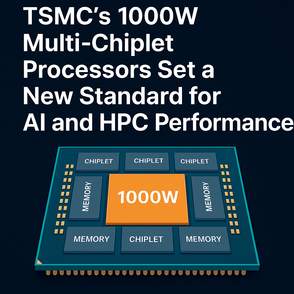
TSMC Unveils 1000W Multi-Chiplet Processors to Redefine AI and HPC Performance at Scale
Taiwan Semiconductor Manufacturing Company (TSMC) is the world’s dominant semiconductor foundry, supplying cutting-edge logic chips for leading tech firms. In Q4 2024, TSMC captured about 67.1% of global foundry revenue, far ahead of second-place Samsung (8.1%). Its unrivaled scale in advanced nodes (5nm, 3nm, etc.) and packaging makes it the cornerstone of the AI and HPC supply chain. For example, TrendForce reports that AI accelerators and high-end smartphones drove strong demand in late 2024, lifting TSMC’s Q4 sales by 14.1% to $26.85 billion. The foundry’s advanced-process capacity is already over-subscribed: sources say 5nm/3nm lines were beyond 100% utilization due to AI/HPC demand in 2024. In short, the industry relies on TSMC to push performance limits – and TSMC’s latest plan for 1000W-class multi-chiplet processors under its new 3DFabric/CoWoS packaging roadmap is poised to reshape AI/HPC hardware.
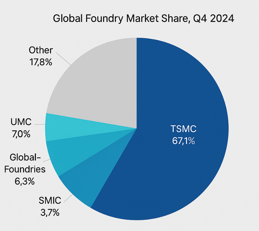
Figure 1: TSMC controls the lion’s share of the global foundry market (≈67% in Q4 2024), dwarfing competitors. This market leadership gives TSMC unparalleled influence over advanced packaging technologies.
Beyond sheer capacity, TSMC’s R&D and manufacturing prowess make it the go-to partner for tech giants. Nvidia, AMD, Apple, and others all use TSMC for their latest chips. TSMC’s integration of high-bandwidth memory (HBM) and multi-die interposers – known as CoWoS (Chip-on-Wafer-on-Substrate) – is already used in products like Nvidia’s H100 GPUs and AMD’s MI300 accelerators. In fact, TSMC reports that current CoWoS interposers can already be up to 2,831 mm² (about 3.3× a single reticle area). Even so, customer demand for more compute is rising faster than ever: AI models and exascale simulations need more cores, memory, and bandwidth than any existing chip can deliver.
TSMC’s response is aggressive scaling of packaging. At its 2025 North America Technology Symposium, TSMC unveiled a 3DFabric roadmap that extends interposer sizes far beyond today’s limits. For example, next-generation CoWoS-L packaging will support up to 4,719 mm² interposers (≈5.5× reticle size) on a 100×100 mm substrate. And TSMC is already planning a 9.5-reticle (≈7,885 mm²) multi-chiplet assembly on a 120×150 mm substrate – roughly the size of a CD case! These “behemoth” chips, TSMC claims, could achieve 40× the compute performance of a standard chip. In short, TSMC’s innovations promise to vastly expand how much silicon and memory a single module can contain, enabling unprecedented performance for AI and HPC.
Chiplet Technology
A Paradigm Shift in High-Performance Computing
Modern high-performance chips are increasingly built from “chiplets” – small dies that are assembled together on a shared package – rather than a single giant monolithic die. Chiplet designs address the limits of monolithic scaling: as chips grow larger, manufacturing yield plunges and costs skyrocket. By partitioning a system-on-chip (SoC) into modular chiplets (e.g. CPU cores, GPU tiles, memory stacks, I/O functions), designers can use smaller dies that are easier and cheaper to fabricate. According to semiconductor analysts, chiplet approaches can improve yield and reduce costs by over 45% compared to monolithic designs. This modularity also creates a broader ecosystem: different vendors can develop standardized chiplets (for compute, memory, AI accelerator engines, etc.) that plug together with open interconnects.
In practice, chiplet architectures deliver several key benefits:
- Scalability: Designers can tile multiple identical chiplets to scale core count or memory. For example, AMD’s latest server CPUs and accelerators use multiple CPU chiplets and memory-on-chiplets linked by a high-speed fabric. This modular tiling allows stacking many cores without making any single die huge.
- Heterogeneous Integration: Chiplets allow mixing different functions or process nodes. A chiplet might integrate a cutting-edge CPU core (5nm) alongside separate 3D-stacked memory or analog I/O chiplets (e.g. made on more mature nodes). This flexibility means each piece can be optimized separately.
- Yield and Cost: Smaller chiplets have much higher manufacturing yield than one giant die. A large die is far more likely to have a defect (and be scrapped), whereas multiple smaller dies can be binned and yields improved. Overall system cost drops because a defect in one chiplet doesn’t ruin the entire multi-chip device.
- Design Reuse and Ecosystem: As SemiEngineering notes, chiplets enable an “open ecosystem of modular components” that can be reused and customized. One chiplet design can serve multiple products, accelerating development and reducing risk. Industry standards like the Universal Chiplet Interconnect Express (UCIe) are emerging to facilitate this interoperability, further fueling chiplet adoption.
- Performance Optimization: Each chiplet can be physically placed to minimize critical interconnect lengths. In advanced packages (2.5D interposers or 3D stacking), chiplets are very close, boosting bandwidth and reducing latency between them. Designs can also include multiple memory chiplets (e.g. stacks of HBM) adjacent to compute chiplets, providing huge on-package memory bandwidth.
These advantages mean chiplets are particularly attractive for AI and HPC chips, where extreme core counts and memory bandwidth are needed. For instance, current AI accelerators often put dozens of cores or GPU tiles on a large interposer with multiple HBM stacks. Without chiplets, a die of that size would be unmanufacturable at good yields. Instead, multi-chip packaging lets Nvidia, AMD, and others combine many units in one package. As one industry analysis put it, chiplets can yield “lower costs, higher performance, and greater flexibility” than monolithic SoCs.
TSMC’s 1000W Multi-Chiplet Processor Architecture
At the heart of TSMC’s initiative are Ultra-Large Multi-Chip Packages. TSMC is extending its CoWoS (Chip-on-Wafer-on-Substrate) packaging technology to support silicon assemblies an order of magnitude larger than today’s standard. The goal is to create single packages containing multiple die stacks and memory for exceptional compute density – even if those packages draw up to 1000 watts or more of power.
Massive Interposers and Substrates
Currently, TSMC’s CoWoS interposers for data-center chips top out around 2,831 mm² – roughly 3.3× a single EUV reticle. That is already being used in products like AMD’s MI300X and NVIDIA’s B200, which combine two logic chiplets with up to eight HBM stacks. But TSMC’s roadmap goes far beyond. By late 2025, the company plans CoWoS-L, supporting interposers up to 4,719 mm² (≈5.5× reticle area) on a 100×100 mm (10,000 mm²) substrate. This next gen package can hold 12 HBM4 stacks plus multiple logic dies, delivering over 3.5× the compute of current designs (enough for GPUs with 12 HBM4 stacks).
That’s just the first step. Looking further out, TSMC will offer interposers up to 7,885 mm² (the “9.5-reticle” size) on a 120×150 mm (18,000 mm²) substrate. For context, a standard CD jewel case is about 142×125 mm, so these chips are enormous. Such a package can integrate four SoIC chiplets (each a stack of a logic die on top of a memory die) along with 12 HBM4 stacks and extra I/O dies. It’s a complete multi-chip superchip. TSMC says these “behemoths” could offer up to 40× the performance of a standard processor, as workload-parallel engines and vast memory banks work in concert.
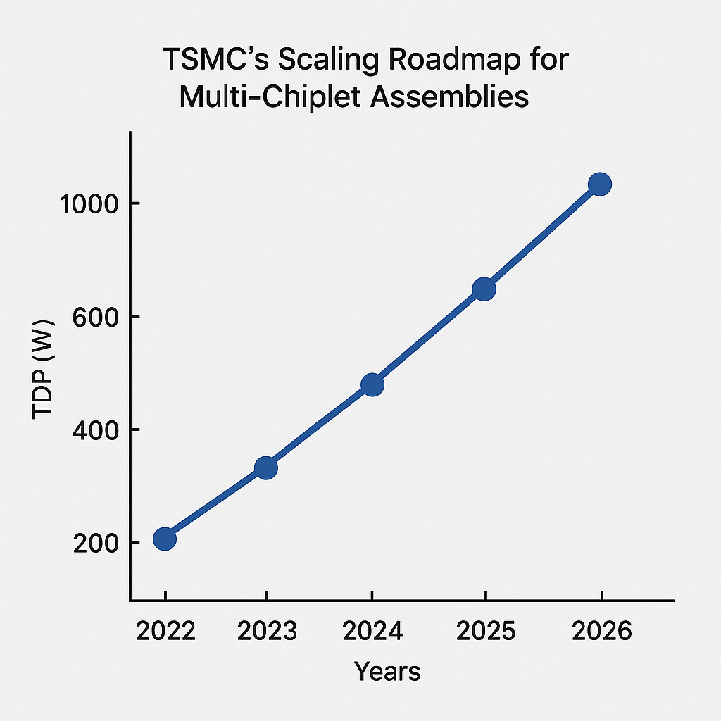
Figure 3: TSMC’s scaling roadmap for multi-chiplet assemblies. Current CoWoS (~2831 mm² interposer) is dwarfed by upcoming CoWoS-L and beyond, culminating in 9.5-reticle (7885 mm²) interposers on 120×150 mm substrates. This drive for larger interposers and substrates enables integration of many chiplets and memory stacks.
Power Delivery Innovations
A key challenge of 1000W-class chips is delivering that much current reliably. Traditional approaches (on-board VRMs and discrete PMICs) would have untenable losses at kilowatt scales. At its 2025 symposium, TSMC outlined a new power delivery strategy: monolithic power management ICs (PMICs) built directly into the package substrate. These PMICs (fabricated on TSMC’s 16nm FinFET) include through-silicon vias (TSVs) and on-wafer inductors, enabling power to be routed through the interposer itself. By placing voltage regulators and inductors inside the chip package, the power pins of the logic die are only millimeters away from the source, greatly reducing parasitic resistance and inductance. TSMC claims this approach can achieve up to 5× higher power delivery density versus conventional board-level VRMs.
Furthermore, the package can embed deep trench capacitors (e.g. DTCs) right into the silicon interposer or substrate. With capacitance densities around 2,500 nF/mm², these capacitors sit directly under the active dies to “smooth out” voltage fluctuations and aid dynamic voltage scaling. In practice, the tightly integrated PMIC+TSV+DTC system allows fine-grained voltage control and rapid transient response at kilowatt loads. This co-design of chip and packaging power infrastructure marks a shift to treating power delivery as part of the silicon design, not an afterthought.
Thermal Design and Cooling
Handling multi-kW heat is another hurdle. A 1000W chip on a board will roast typical air-cooled designs. Even conventional liquid cooling (cold plate + coolant) is reaching its limits. As Tom’s Hardware notes, these large multi-chip modules “generate an enormous amount of heat”, forcing designers to explore direct liquid cooling or immersion cooling. (NVIDIA already uses such advanced cooling for its highest-end data-center GPUs.) TSMC itself can’t solve facility-level cooling, but it acknowledges system integrators must. In practical terms, deploying TSMC’s 1000W chiplets will likely mean custom rack designs with cooled cold plates or immersion tanks to remove heat efficiently.
The packaging form factor also strains current standards. The 100×100 mm substrate is near the limit of OCP OAM 2.0 (102×165 mm). At 120×150 mm, the new substrate exceeds existing module footprints. The industry may need new module form factors or board layouts to accommodate these chips. For now, TSMC appears focused on the silicon and package; server designers will have to innovate on enclosures and cooling.
Aggregate Performance and Scaling
Putting it all together, what does a 1000W TSMC chip look like? Imagine a single package containing tens of billions of transistors. For example, four 3D-stacked SoIC chiplets, each combining a next-gen CPU/GPU core-stack on top of HBM memory, along with 12 separate HBM4 stacks. This could easily provide thousands of CPU cores or GPU cores, and terabytes of on-package memory bandwidth. TSMC’s performance claim – up to 40× more than a “standard processor” – reflects this massive parallelism. Even if some of that is architectural scaling, the combination of sheer compute elements and memory throughput would be unprecedented. In effect, TSMC is offering a wafer-scale-in-package solution short of actually making a single-wafer chip.
These innovations – larger interposers, integrated PMICs, and 3D SoIC stacking – give TSMC a lead in raw packaging capability. Its competitors have their own approaches (Intel’s EMIB/Foveros, for instance) but none have announced anything close to 9.5-reticle packaging yet. Importantly, TSMC’s strategy is flexible: it can incrementally bring out CoWoS-L (4,719 mm²) by next year, then push to the 9.5-reticle designs afterward, as customers’ products mature. For chip designers, this means one foundry (TSMC) can take them from today’s multi-chip products straight to kilowatt-class systems without changing wafer suppliers or fundamental flow.
Market Implications and Competitive Landscape
TSMC’s 1000W chiplet strategy has huge ramifications for the AI/HPC market. By far the biggest beneficiaries in the near term will be companies that rely on TSMC for leading-edge dies – notably Nvidia, AMD, and specialized AI silicon firms. Nvidia, for example, has already signaled a shift to TSMC’s CoWoS-L packaging for its next-gen Blackwell GPUs. CEO Jensen Huang confirmed Nvidia will “move largely to CoWoS-L” for Blackwell, increasing capacity there while phasing out CoWoS-S. In effect, Nvidia is aligning with TSMC’s roadmap, anticipating its new GPUs will use those larger interposers and substrates. For AMD, its forthcoming MI300X accelerators (used in current DOE supercomputers) already exploit two chiplets on a CoWoS substrate. One can expect AMD’s future CDNA generations to use even larger 3DFabric packages with more chiplets and HBM, tapping directly into TSMC’s capabilities.
By contrast, Intel is racing to keep up but via different paths. Intel has developed its own multi-die packaging (EMIB, Foveros), but so far these have targeted lower-power designs (e.g. Alder Lake mobile CPUs, Ponte Vecchio GPUs). Intel has announced some wafer-scale experiments, but no public plan matches TSMC’s 9.5-reticle product. In the AI GPU space, Intel’s recent designs (like Xe-LP) play catch-up to Nvidia and AMD. Intel also lacks a high-volume foundry operation on par with TSMC, so it may eventually need to partner (or outsource) for the highest-end chips. AMD of course also uses TSMC fabs for its logic; it too has collaborated with TSMC (and with UMC/TSMC) on memory-on-package (e.g. HBM3 for MI300). In any case, AMD and Nvidia have effectively outsourced their chip fabrication (and now packaging roadmap) to TSMC, meaning TSMC’s roadmap strongly influences their product roadmaps.
Market analysts see this dynamic clearly. TrendForce notes that AI and high-performance computing are polarizing the foundry market: “Chipmakers like TSMC, which specializes in high-end IC production, rode the waves of emerging technologies including AI and HPC devices.” In Q4 2024, TSMC’s foundry share jumped to 67.1% on strong AI server demand, while Samsung fell further behind. Another analyst observed that TSMC’s 67.1% share (up from 64.7%) widened the gap with Samsung to 59 points. The upshot is that TSMC’s leadership in packaging directly translates into its ability to win business for next-gen AI chips.
TSMC’s new 1000W class chips put pressure on competitors’ strategies. For example, NVIDIA moving to CoWoS-L implies wafer slots will migrate to even more expensive packaging. TSMC’s roadmap may also influence customers like Google or Cerebras: the tech giant Google, building its own TPU and AI accelerators, could leverage TSMC’s technology rather than designing a custom wafer-scale chip (like Tesla’s Dojo). (Indeed, TSMC notes that Tesla’s Dojo currently uses wafer-level integration – a method TSMC offers as SoW-X – but TSMC expects more customers beyond Cerebras and Tesla in future.) Meanwhile, European and Chinese chipmakers are watching closely. TSMC’s advances raise the bar: to compete, they must develop equivalent packaging or design specialization.
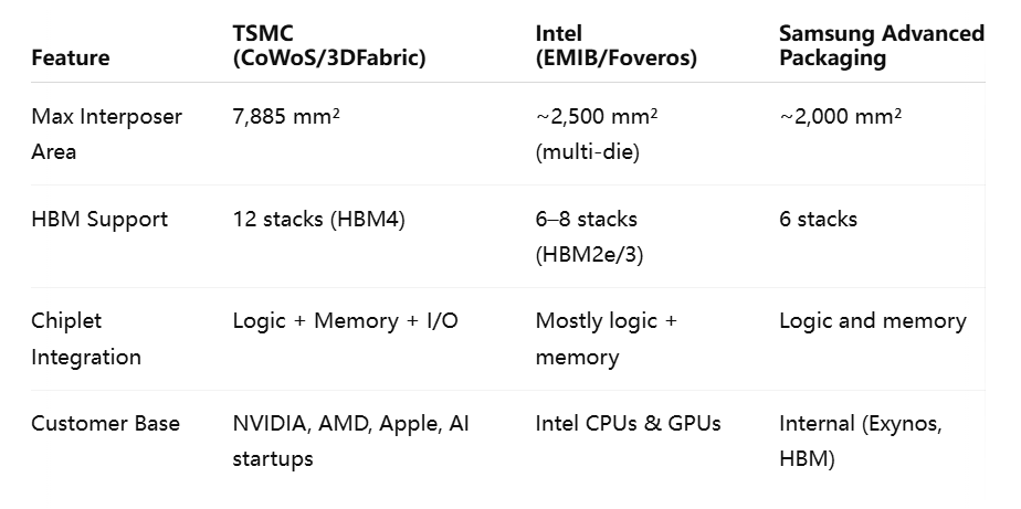
Below is a competitive comparison:
Analysts from firms like Gartner and TrendForce echo this: demand for AI semiconductors is skyrocketing (forecast to reach ~$71 billion in 2024), and growth is centered on advanced-node, high-memory solutions. In other words, the market is racing towards TSMC’s turf. As a Focus Taiwan report notes, “with the global foundry business increasingly polarized, chipmakers like TSMC… rode the waves of… AI and HPC devices.”. By accelerating its 1000W chip development, TSMC is essentially betting that its customers will invest in these mega-modules, further entrenching its position.
Future Outlook
The implications of TSMC’s 1000W chiplet leap extend deep into future computing trends. On the use case side, these processors target the very top of the performance pyramid. Expect them in:
- AI Supercomputers: Training the largest machine-learning models (e.g. massive LLMs or foundational models) requires enormous parallel compute. A 1000W chiplet could power one “node” of a training cluster, providing >1000 cores (CPU or GPU) plus terabytes of HBM. As generative AI adoption surges (data centers now routinely deploy tens of thousands of GPUs), the need for single-chip solutions that can handle extreme workloads grows.
- Exascale HPC: The world’s exascale systems (like Frontier and Aurora) already use accelerators, but upcoming generations (2026+) will push even harder on performance per rack. Systems designers might use TSMC’s new chips in future exascale bids, harnessing their high FLOPS/Watt and integrated memory to simplify scaling.
- Large-Scale Simulations: Scientific applications (climate modeling, genomics, physics) often run on top-tier HPC. A chip that can pack many memory-stacked cores in one package will accelerate these tasks, especially as on-node memory bandwidth becomes a bottleneck in traditional clusters.
- AI Cloud and Inference: Even inference of large models in cloud data centers could benefit. While inference tasks often have lower batch sizes, the sheer model size (billions of parameters) demands high memory capacity; a chip with huge on-package HBM could host entire models without off-chip memory.
Regarding timelines, TSMC’s own statements suggest a phased roll-out. Its CoWoS-L (100×100 mm, 4,719 mm² interposer) is slated for about “next year, or a bit later” (2025). That generation alone boosts performance ~3.5× over current designs, likely hitting the market in the 2025–2026 timeframe. The even larger 9.5-reticle packages (7885 mm²) seem aimed at the late-2020s (possibly 2026–2027). These timelines align with customer roadmaps: Nvidia’s Hopper/H100 series will transition to Blackwell (2025–26), AMD’s next accelerators will appear around 2026, and new AI startups will be taking delivery of advanced chips.
Analyst commentary underscores the urgency. An industry source cited projections of a “TDP explosion” in AI chips: typical accelerator power envelopes were 200–300W a few years ago, but are “heading to 1000 watts and beyond within a few years”. Companies like NVIDIA and Intel engineers openly discuss designing chips in the multi-kilowatt per rack range. In short, the hardware world is bracing for a multi-kW-per-chip future – exactly the niche TSMC’s new tech is built for.
Of course, realizing this future depends on the ecosystem adapting. Data centers must upgrade infrastructure (power delivery, cooling, racks) to host kilowatt chips. Early adopters (hyperscalers, national labs) will likely pave the way. We may see initial deployments in dedicated AI racks or specialized HPC cabinets with liquid cooling loops. Over time, as confidence grows, these chips could become mainstream for any workload that benefits from extreme parallelism (even beyond AI, such as cryptography, big data analytics, etc.).
Lastly, beyond immediate use cases, TSMC’s move could influence broader trends. It may accelerate the shift to heterogeneous computing: chips combining CPUs, GPUs, TPUs, and other accelerators on one package become viable. It may spur further investment in optical or other advanced interconnects to handle off-chip communication (since off-package links might become the new bottleneck once one package is full). Even Moore’s Law could get a boost: multi-chip integration sidesteps reticle limits, so performance can grow even as transistor scaling slows.
In summary, TSMC’s 1000W multi-chiplet processors are not just a spec sheet novelty – they represent a leap in system design. By enabling a single silicon assembly to rival a small cluster in compute power, TSMC is revolutionizing what “a processor” means. For AI and HPC, that means faster training of larger models, more capable supercomputers, and possibly new architectures of computing clusters. Investors and industry watchers should note: the platform for tomorrow’s AI and HPC is being built today, and TSMC is laying the foundation.
Conclusion
TSMC’s 1000W multi-chiplet processors represent the next evolutionary step in high-performance computing and AI acceleration. With record-breaking interposer sizes, tightly integrated power delivery, and extreme on-package memory bandwidth, these processors redefine what a “chip” can be.
In a world where AI training times, data volumes, and model parameters are growing exponentially, TSMC has placed itself at the center of the AI/HPC revolution. The future of computing is no longer just about faster transistors—it’s about smarter system architecture, modular design, and gigantic, power-hungry packages that redefine the limits of silicon.
References
- TSMC Official 3DFabric & CoWoS Packaging Overview
https://www.tsmc.com/english/dedicatedFoundry/technology/3DFabric - TSMC Reveals Massive 1000W AI Chip Packaging Plan
https://www.tomshardware.com/tech-industry/tsmc-multi-chip-packaging - The Rise of Multi-Chiplet Architectures in HPC
https://www.anandtech.com/show/ai-hpc-chiplets-analysis - TSMC Dominates Global Foundry Market
https://www.trendforce.com/presscenter/news/20240402-TSMC - Chiplet Economics and Design Trends
https://semiengineering.com/chiplets-take-center-stage - Inside the Power-Hungry Future of AI Hardware
https://www.theverge.com/tech/ai-chip-tsmc-1000w - Co-Packaged Optics and Power Delivery Challenges
https://spectrum.ieee.org/co-packaged-optics-ai-chips - Semiconductor Market and AI Growth Trajectories
https://www.mckinsey.com/industries/semiconductors/insights/ai-chips - NVIDIA’s Shift to TSMC CoWoS-L for Blackwell GPUs
https://www.reuters.com/technology/nvidia-tsmc-packaging - TSMC Expands CoWoS Capacity Amid AI Boom
https://focustaiwan.tw/business/tsmc-ai-chip-packaging