
MicroLED: The Next Great Leap in Display Technology and Its Path to Market Disruption
In the ever-evolving landscape of consumer electronics and visual technologies, the demand for high-performance, energy-efficient, and visually immersive displays has never been more pronounced. From smartphones and televisions to augmented reality (AR) headsets and automotive dashboards, display technology forms the visual foundation of the modern digital experience. Amidst this backdrop, MicroLED technology has emerged as a highly promising next-generation solution—positioned to not only challenge incumbent technologies such as OLED and LCD but to fundamentally reshape the display industry’s technical and commercial paradigms.
MicroLED, or micro light-emitting diode, refers to a class of displays composed of millions of microscopic inorganic LEDs—each capable of emitting its own light and color. Unlike LCDs that require backlighting, or OLEDs that rely on organic compounds prone to burn-in and degradation, MicroLEDs offer self-emissive, inorganic, and highly durable pixel architectures. The result is a display that is brighter, more energy-efficient, longer-lasting, and capable of achieving superior contrast ratios and color fidelity. These attributes make MicroLEDs highly suitable not only for consumer electronics but also for professional-grade displays, medical visualization, automotive instrumentation, and future-forward wearables.
The strategic importance of MicroLED extends beyond its visual performance. Its modular and scalable design allows for flexible screen configurations, from ultra-small wearables to enormous multi-panel video walls. This scalability, combined with its robustness and ambient visibility, has attracted attention from technology giants including Apple, Samsung, Sony, and LG—each investing heavily in R&D, pilot production lines, and intellectual property portfolios aimed at securing early leadership in a potentially transformative market.
Despite these advantages, the path to widespread adoption is neither straightforward nor guaranteed. The manufacturing complexity of MicroLEDs—particularly the transfer and alignment of millions of microscopic LED chips onto a backplane—presents a significant technical barrier. Moreover, high production costs and relatively low yield rates currently restrict commercial viability to premium product categories.
This blog post provides an in-depth exploration of MicroLED technology, assessing its underlying scientific principles, comparative performance metrics, investment landscape, current applications, and commercialization challenges. The analysis includes two informative charts and one comparative table to illustrate key technical and market developments. Together, these components aim to provide technology executives, investors, engineers, and industry analysts with a comprehensive understanding of how and why MicroLED is poised to revolutionize the display industry in the years ahead.
The Science and Structure of MicroLED
MicroLED technology represents a significant leap forward in display innovation, fundamentally rethinking how light is generated, managed, and perceived at the pixel level. While it shares the self-emissive nature of OLED, MicroLED is differentiated by its use of inorganic materials, advanced manufacturing techniques, and unmatched scalability across a wide range of display sizes and use cases. This section examines the fundamental science and architecture of MicroLEDs, comparing their performance against competing technologies, and analyzing the implications for future device design and manufacturing.
MicroLED Fundamentals: Pixel-Level Light Emission
At the core of MicroLED displays lies the principle of self-emissive light generation, whereby each pixel—or subpixel—is composed of a microscopic light-emitting diode capable of producing red, green, or blue light. These microscopic LEDs are fabricated from gallium nitride (GaN) or similar inorganic materials, known for their high luminous efficacy, thermal stability, and long operational lifespan.
Unlike LCDs, which rely on a backlight passing through liquid crystal layers and color filters, or OLEDs, which utilize organic electroluminescent compounds, MicroLEDs emit light directly and independently. This results in displays with unparalleled brightness, contrast, and color precision, while also eliminating issues such as motion blur, color washout, and backlight bleed.
Each MicroLED subpixel is driven by its own thin-film transistor (TFT), integrated into a silicon, glass, or flexible backplane. The absence of backlighting not only reduces energy consumption but also enables thinner display profiles and greater design flexibility—qualities increasingly demanded in next-generation consumer devices.
Material and Structural Advantages
The primary materials used in MicroLEDs—typically GaN for blue and green, and aluminum indium gallium phosphide (AlInGaP) for red—offer several inherent advantages over organic compounds. These include:
- High brightness capacity, exceeding 1,000 to 10,000 nits, making MicroLEDs ideal for outdoor and high-ambient light environments.
- Exceptional thermal efficiency, allowing for prolonged operation without thermal degradation.
- Longer lifespan, with operational endurance surpassing 100,000 hours—nearly double that of OLED.
- Higher pixel density, enabling resolutions beyond 2000 PPI (pixels per inch), which is particularly advantageous for AR/VR applications.
The use of inorganic materials also drastically reduces the risk of burn-in and image retention, a known limitation of OLED displays subjected to static content over time.
Comparison with Competing Technologies
To appreciate the disruptive potential of MicroLEDs, it is essential to compare their performance characteristics with those of incumbent display technologies. LCD and OLED displays each have their strengths but are fundamentally constrained by their reliance on either transmissive layers (in the case of LCDs) or organic emissive elements (in OLEDs).
LCDs, while cost-effective and ubiquitous, suffer from limitations in contrast ratio, viewing angles, and response time. OLEDs improve upon these parameters but introduce trade-offs in terms of material longevity, peak brightness, and susceptibility to image retention.
MicroLEDs overcome these limitations by offering the best aspects of both technologies—superior contrast and viewing angles with the added benefits of inorganic durability and power efficiency. The result is a display technology that promises not only incremental improvement but category-defining advancement.
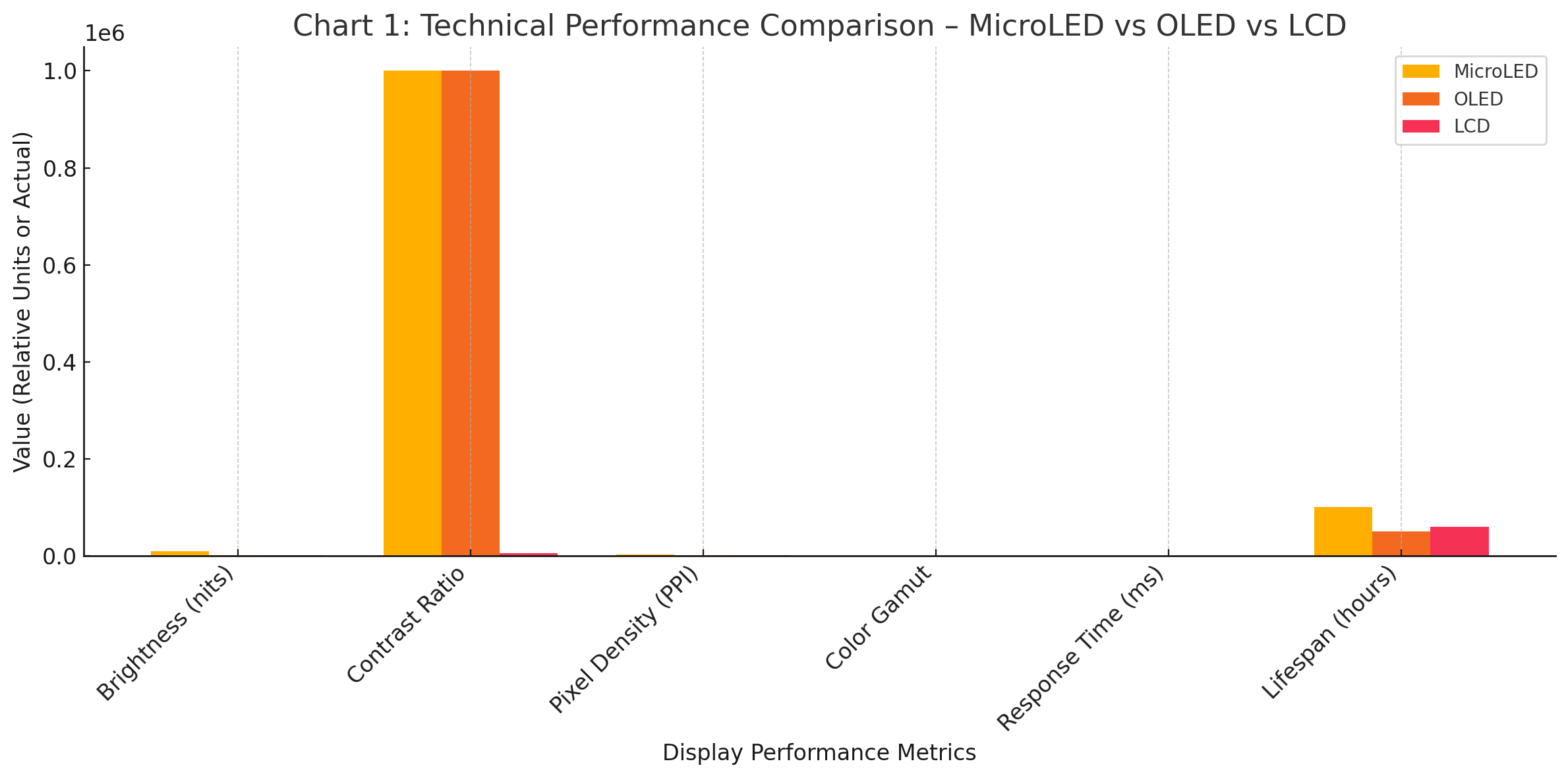
This comparison underscores MicroLED’s capacity to combine the aesthetic superiority of OLED with the reliability and scalability of LCD, while introducing entirely new dimensions in performance.
Fabrication Process: A Key Bottleneck
While the theoretical advantages of MicroLEDs are substantial, the fabrication process remains a formidable obstacle to mass production. MicroLED manufacturing involves multiple high-precision steps:
- Epitaxial growth of LED wafers (typically on sapphire or silicon substrates)
- Micro-LED chip dicing to create individual emitters
- Mass transfer of millions of LED chips onto the backplane with micron-level accuracy
- Bonding and interconnection to enable active matrix addressing
- Color conversion or mixing, especially for RGB integration
- Final encapsulation and inspection
Among these, the mass transfer process—responsible for placing and aligning millions of microscopic LED chips—is widely recognized as the principal technical bottleneck. Yield rates, placement accuracy, and throughput remain challenges that hinder the scalability of MicroLED fabrication.
Several solutions are being explored, including laser-assisted transfer, elastomer stamp transfer, electrostatic placement, and monolithic integration, each with varying trade-offs in cost, complexity, and performance.
Integration with Emerging Applications
MicroLED’s ability to operate efficiently in a wide range of form factors makes it an ideal candidate for future device categories. Key application areas currently under active exploration include:
- AR/VR displays requiring ultra-high resolution and low latency
- Smartwatches and fitness trackers demanding high brightness and low power
- Large-format displays for retail, public venues, and home theater
- Automotive dashboards and heads-up displays (HUDs) that must perform reliably across lighting conditions
MicroLED’s modularity also enables novel screen geometries, including bezel-less tiling, curved surfaces, and transparent panels—further expanding design possibilities.
MicroLED technology represents a convergence of advanced materials science, semiconductor engineering, and display innovation. With superior brightness, efficiency, and durability, it addresses many of the limitations faced by current-generation displays. While technical hurdles remain—particularly in manufacturing—the performance potential of MicroLED is indisputable. As we transition to the next section, we will shift focus from the technological underpinnings to the market forces and investment dynamics driving the global push toward MicroLED commercialization.
Market Dynamics and Investment Trends
The emergence of MicroLED technology is not merely a technical innovation—it is also a strategic inflection point in the global display industry. With potential applications ranging from ultra-premium televisions to energy-efficient wearables and high-resolution AR/VR headsets, MicroLED is attracting significant investment, competitive maneuvering, and cross-industry collaboration. This section examines the current state of the MicroLED market, outlines key investment trends, profiles major industry players, and explores the long-term commercial outlook for this transformative display technology.
Global Investment Landscape
Over the past decade, investment in MicroLED R&D and pilot production has increased markedly, as firms position themselves for early leadership in what is projected to be a multi-billion-dollar market. According to industry estimates, the global MicroLED display market is expected to reach USD 20–30 billion by 2030, driven by rapid commercialization in consumer electronics, automotive, industrial, and medical applications.
These investments are not only focused on final display products but also span the entire value chain, including:
- Epitaxial wafer production
- Chiplet transfer and bonding equipment
- Inspection and repair technologies
- Backplane integration
- Color conversion and pixel encapsulation
Countries such as South Korea, the United States, and China have emerged as innovation hubs, each pursuing national strategies that integrate MicroLED as part of broader display and semiconductor initiatives.
Major Players and Strategic Roadmaps
Several established technology giants are heavily invested in MicroLED development, each targeting different applications and market segments. These firms are not only racing to overcome manufacturing challenges but also to secure intellectual property (IP) dominance and early brand association with MicroLED innovation.
Samsung Electronics
Samsung is arguably the most prominent corporate proponent of MicroLED, having showcased its “The Wall” modular TV series as a premium use case for large-scale, bezel-less displays. The company has invested in developing scalable transfer technologies and high-yield fabrication processes, with plans to bring MicroLED into smaller form factors, including televisions under 77 inches.
Apple Inc.
Apple has pursued a long-term strategy aimed at integrating MicroLED into future Apple Watch and AR/VR products. In 2014, it acquired LuxVue, a MicroLED startup with expertise in low-power applications. Apple has since built internal MicroLED development facilities in California and Taiwan, with supply chain partnerships in place to support eventual commercialization.
Sony Corporation
Sony was the first company to launch a commercial MicroLED display product—its Crystal LED (CLED) system. While currently limited to professional and signage markets, Sony continues to refine the technology, aiming for future crossover into consumer-facing devices.
LG Display, AUO, BOE Technology, and others
These firms are also actively pursuing MicroLED, often in collaboration with startups, universities, and equipment vendors. While most are at the pilot or demonstration stage, their involvement signals broad industry consensus on MicroLED’s disruptive potential.
Emerging Innovators and IP Ecosystem
Alongside established players, a vibrant ecosystem of startups and research institutions is contributing to the MicroLED innovation pipeline. Companies such as PlayNitride (Taiwan), VueReal (Canada), and Rohinni (U.S.) are developing novel manufacturing methods, including inkjet printing, roll-to-roll fabrication, and microchip stamping techniques.
Universities and national labs have also emerged as crucial collaborators, supported by government grants targeting advanced manufacturing, semiconductor innovation, and next-generation display systems. The aggregation of patents in areas such as chip transfer, mass alignment, defect detection, and flexible substrates suggests that IP ownership will play a central role in shaping the competitive dynamics of the MicroLED market.
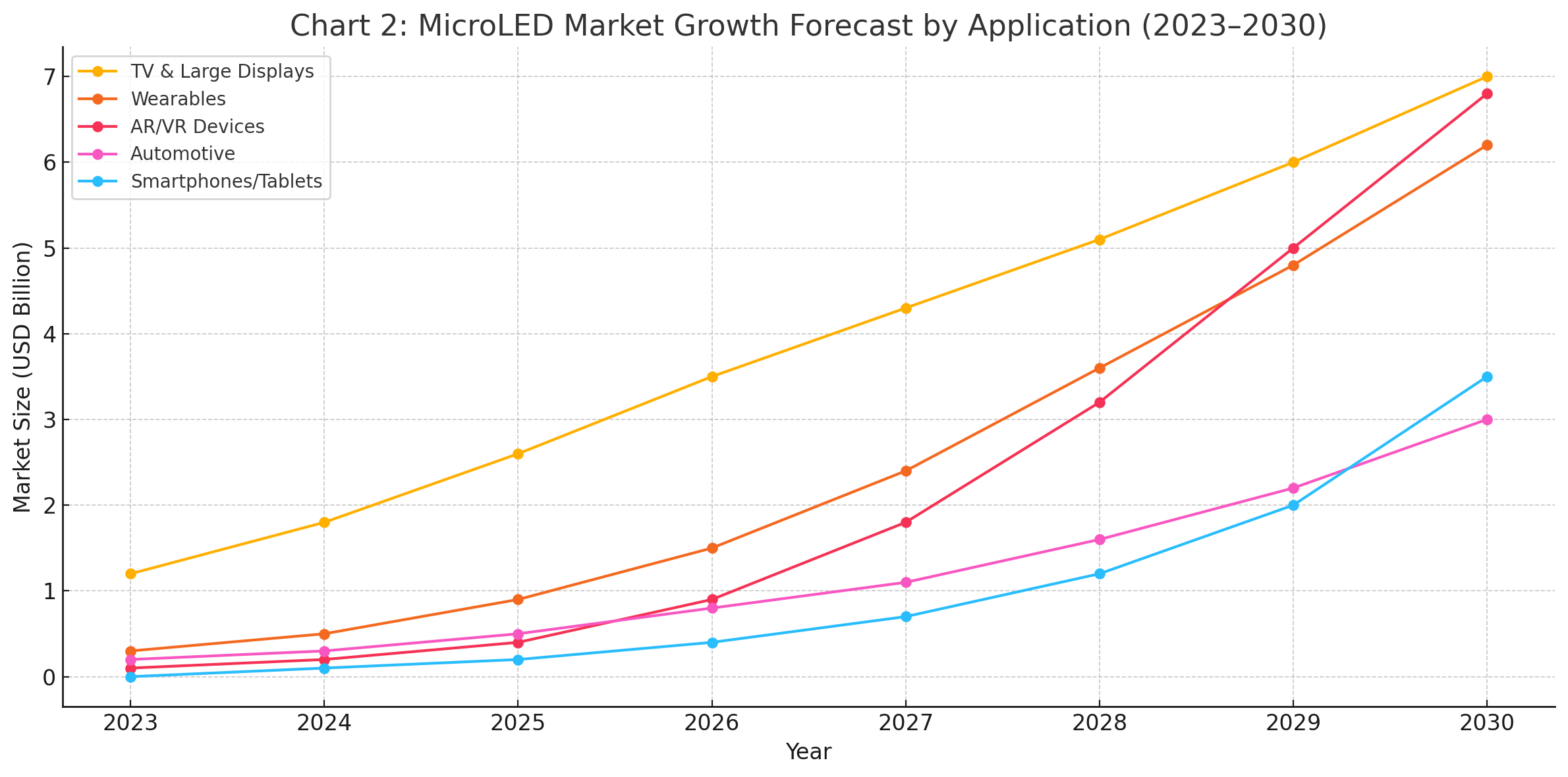
Market Growth Forecast and Projections
To better understand the commercial trajectory of MicroLED, consider the projected market growth across application segments. The technology’s adoption is expected to follow a tiered path: beginning with high-end commercial installations, followed by premium consumer electronics, and eventually penetrating mass-market applications.
This line chart tracks projected market size (in USD billions) for key MicroLED application segments between 2023 and 2030, including:
- Large-format displays (TVs, signage)
- Wearables (smartwatches, fitness bands)
- AR/VR (headsets, HUDs)
- Automotive (instrument clusters, HUDs)
- Smartphones and tablets
Strategic Capital Deployment
As commercialization accelerates, companies are making substantial capital expenditures to develop or expand pilot production lines. These investments are intended to increase yield, precision, and throughput, while reducing the high unit costs that currently limit MicroLED to luxury applications.
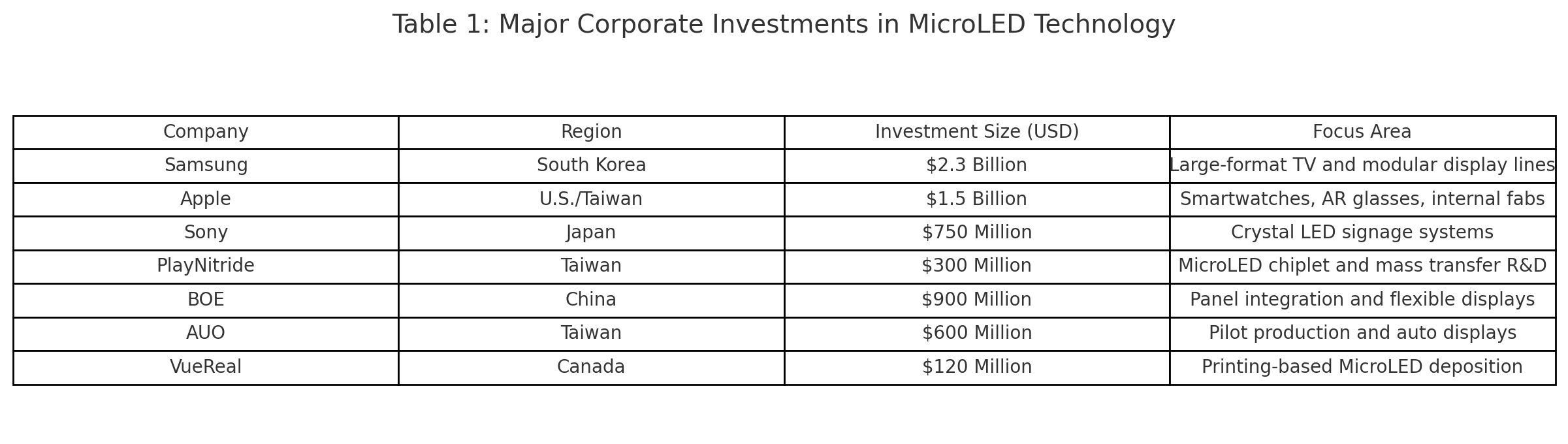
This table reflects the global and multi-dimensional nature of MicroLED investment. Notably, significant funding is flowing not just into end-product development but also into equipment innovation, process automation, and vertical integration strategies.
Supply Chain Considerations
A robust and vertically aligned supply chain is essential for scaling MicroLED. Presently, several chokepoints persist:
- Wafer scalability: Limited availability of large, defect-free GaN wafers
- Mass transfer bottlenecks: Low throughput in pick-and-place or stamp-based assembly
- Inspection and repair costs: High expense associated with identifying and correcting pixel-level defects
- Backplane technology: Lack of standardized integration with flexible or high-speed TFT backplanes
To address these issues, companies are investing in automation, AI-assisted inspection, and hybrid bonding technologies, aimed at increasing yield and reducing costs over time.
Long-Term Commercial Viability
The path to mainstream adoption of MicroLED technology will depend on the industry’s ability to lower production costs, streamline transfer techniques, and improve yield consistency. Analysts forecast that meaningful price parity with OLED may not occur until 2027–2028, by which time improved economies of scale and hybrid integration processes are expected to mature.
However, MicroLED’s energy efficiency, lifespan, and visual superiority offer enough long-term value to justify early investment—particularly in segments where display performance is a core differentiator. From luxury TVs and fitness wearables to HUDs and immersive headsets, MicroLED will likely follow a premium-to-mainstream adoption curve.
MicroLED technology stands at the convergence of scientific innovation and market opportunity. As investment capital continues to flow, strategic partnerships deepen, and fabrication capabilities improve, MicroLED is steadily progressing from laboratory curiosity to commercial reality.
Industry Applications and Emerging Deployments
While MicroLED technology is still in the early stages of mass commercialization, it has already begun to assert its influence across a diverse set of industries. Its unique combination of ultra-high brightness, pixel-level light control, energy efficiency, and longevity makes it particularly attractive for high-end use cases that demand uncompromising performance. As the technology matures and cost structures evolve, MicroLED is expected to transition from niche deployments to broader market adoption. This section explores current and emerging applications of MicroLED displays, highlighting how leading industries are deploying the technology to address both functional and experiential challenges.
Premium Televisions and Large-Format Displays
The most prominent and visible deployment of MicroLED to date has been in the premium television and commercial signage market. This is due to two primary reasons: the relative flexibility of display size and power consumption at scale, and the premium margins available in luxury product segments.
Samsung's “The Wall” is the most notable commercial product leveraging MicroLED. Initially launched for commercial and ultra-premium home installations, this modular, bezel-free display system allows for customizable screen sizes, reaching over 100 inches with 4K and 8K resolution capabilities. The display panels are composed of MicroLED tiles that can be seamlessly combined, creating a near-infinite canvas. Samsung has positioned this product not only as a high-end entertainment solution but also as a commercial display system for venues such as airports, galleries, and corporate lobbies.
Sony's Crystal LED (CLED) also deserves mention. Although initially targeted at professional broadcasting and cinema-grade installations, CLED has begun penetrating the retail signage and architectural visualization markets. With unparalleled black levels, color uniformity, and viewing angles, MicroLED displays like CLED are establishing a new benchmark for visual fidelity in large-screen deployments.
Despite the current premium pricing, these deployments act as strategic flagships—demonstrating the technology’s capability while supporting incremental improvements in manufacturing processes and supply chain coordination.
Smartwatches and Wearables
Perhaps the most closely watched frontier for MicroLED integration is in the wearables market, particularly smartwatches and fitness bands. These devices are ideal candidates for MicroLED adoption due to their stringent requirements for power efficiency, sunlight readability, and form factor miniaturization.
Apple’s rumored transition from OLED to MicroLED for future iterations of the Apple Watch exemplifies the industry's direction. By leveraging MicroLED’s higher brightness and lower power draw, wearables can significantly improve battery life and outdoor performance—two of the most cited pain points in current-generation devices.
Moreover, the thinness and mechanical flexibility of MicroLED modules support curved and edge-to-edge designs, allowing device manufacturers to expand screen real estate without increasing physical footprint. The superior durability of MicroLED, particularly its resistance to burn-in, makes it especially attractive for always-on display (AOD) modes common in health and fitness monitoring applications.
As pilot production improves and unit costs decline, the integration of MicroLED into wearables is expected to be one of the first mass-market inflection points for the technology.
Automotive Displays and Human-Machine Interfaces (HMIs)
The automotive sector is emerging as a critical growth area for MicroLED, driven by the rapid evolution of in-vehicle infotainment systems, heads-up displays (HUDs), and digital instrument clusters. These applications require displays that are not only high resolution but also capable of operating under variable lighting conditions, including direct sunlight and low-visibility environments.
MicroLED’s high contrast ratio and exceptional brightness levels—often exceeding 5,000 nits—make it ideally suited for such environments. Furthermore, its long lifespan and thermal stability enhance operational reliability in automotive-grade conditions, where fluctuations in temperature and vibration tolerance are critical factors.
Several automakers and tier-one suppliers have initiated joint development programs to explore MicroLED integration into curved dashboard displays, rearview mirror replacements, and passenger entertainment systems. Additionally, transparent MicroLED displays are under development for next-generation windscreen HUDs, promising to enhance driver situational awareness without compromising visibility.
Given the increasing digitalization of the cockpit, MicroLED offers a compelling combination of design freedom, safety, and visual clarity.
Augmented Reality (AR), Virtual Reality (VR), and Mixed Reality (MR)
The AR/VR sector presents perhaps the most demanding use case for display technologies—requiring ultra-high resolution (to avoid the screen-door effect), low latency, high brightness, and compact form factors that can be integrated into head-mounted displays (HMDs). MicroLED is uniquely positioned to address all of these challenges.
In AR applications, particularly in outdoor settings, OLEDs often struggle with peak brightness, making virtual overlays hard to read. MicroLED displays, by contrast, offer luminance levels far in excess of OLED, ensuring visibility even in direct sunlight. Their extremely fast response time—measured in microseconds—also ensures latency-free interactions, which is essential for immersive experiences and motion tracking.
Further, MicroLED’s ability to achieve pixel densities exceeding 2000 PPI makes it possible to build compact, high-resolution microdisplays. Startups and university labs are working on micro-projectors and waveguide-integrated displays based on MicroLEDs, which could form the basis for lightweight AR glasses and next-generation MR headsets.
Although commercial deployment in this sector remains limited, MicroLED is widely regarded as the display technology of choice for the future of immersive computing.
Commercial Signage, Retail, and Public Display Systems
MicroLED displays are increasingly being explored for commercial signage and public information systems, where performance, modularity, and maintenance are key considerations. These include:
- Retail environments, where vibrant displays can drive customer engagement
- Transportation hubs, such as airports and train stations, where high reliability and 24/7 operation are mandatory
- Outdoor billboards, where resistance to weather and long-term image stability are critical
In these applications, MicroLED's advantages in color uniformity, weather resistance, and serviceability are significant. Additionally, the modular construction of large-scale MicroLED panels allows for easier installation and repair, making them cost-effective over longer time horizons despite higher upfront investment.
As competition intensifies in the retail and out-of-home advertising sectors, the ability to deliver differentiated visual experiences will be a key value proposition for MicroLED-equipped installations.
Prototype Deployments vs. Commercial Availability
Despite the growing number of announcements and demonstrations, it is important to distinguish between prototype-level integration and full commercial availability. Many of the MicroLED applications discussed above are still in various stages of pilot production or limited-market rollout. Key barriers include:
- Low manufacturing yield, especially at small pixel pitches
- High production costs, resulting in limited affordability
- Lack of mature supply chains, particularly for driver ICs and transfer equipment
- Design complexity associated with integrating MicroLEDs into curved or flexible substrates
Nonetheless, the technology readiness level (TRL) is steadily rising. Industry observers note that MicroLED is now where OLED was a decade ago—in transition from experimental platforms to early-stage commercialization, particularly in premium product categories.
The spectrum of current and emerging MicroLED deployments illustrates the technology’s versatility and broad market potential. From ultra-luxury televisions and AR headsets to automotive dashboards and wearable displays, MicroLED is redefining what is technically and experientially possible. While cost and manufacturing barriers persist, the growing list of real-world applications signals that MicroLED is moving from theoretical superiority to practical implementation.
Challenges and Roadblocks to Mass Adoption
Despite its significant promise and a growing number of prototype demonstrations and niche deployments, MicroLED technology remains far from mass-market penetration. While the performance metrics of MicroLED displays are widely acknowledged to surpass those of current display technologies, the pathway to scalability is obstructed by an array of technical, economic, and structural challenges. This section examines the major roadblocks impeding widespread MicroLED adoption and highlights the critical areas where innovation and industrial collaboration are essential for unlocking commercial viability.
Manufacturing Complexity and Transfer Yield Bottlenecks
The most pressing challenge in MicroLED commercialization lies in the mass transfer and assembly process. Unlike OLED or LCD technologies that are built up layer by layer through printing or deposition techniques, MicroLED displays require the precise placement of millions of microscopic LED chips—each measuring only a few micrometers in diameter—onto a target substrate with sub-micron alignment accuracy.
The leading transfer technologies include:
- Elastomer stamp transfer, where a stamp lifts and deposits LED arrays from a donor wafer
- Laser-assisted transfer, using optical pulses to detach chips and place them on a receiver substrate
- Fluidic assembly and electrostatic techniques, under investigation for batch processing
Each method presents a trade-off between throughput, placement precision, and cost. To manufacture a full-HD or 4K MicroLED display, tens of millions of RGB subpixels must be transferred with near-perfect accuracy. Even a 99.99% success rate results in thousands of defective pixels, necessitating additional repair steps such as redundant subpixel replacement or pixel-level redundancy schemes.
These technical demands have hindered the development of high-yield, high-throughput production lines, effectively limiting MicroLED production to small displays or low-volume premium segments.
Cost Constraints and Capital Expenditures
Manufacturing difficulties directly translate into high per-unit production costs, which currently prevent MicroLED from competing with LCD or OLED in most consumer applications. According to industry estimates, the cost of producing a MicroLED panel at similar scale remains 5–10 times higher than OLED for comparable resolutions and screen sizes.
Key cost drivers include:
- Epitaxial wafer fabrication, especially for defect-free GaN substrates
- Chip dicing and sorting equipment with sub-micron precision
- Mass transfer tooling, still in the early stages of industrial maturity
- Inspection and defect-repair systems, needed to identify and correct misaligned or non-functioning pixels
In addition, investment in MicroLED fabrication lines requires significant capital expenditures, with pilot production lines ranging from $200 million to $500 million depending on scale and vertical integration. For many display manufacturers, particularly those outside the top tier, these costs present a substantial barrier to entry.
Until new manufacturing paradigms—such as monolithic integration or quantum dot-assisted color conversion—are industrialized, MicroLED will likely remain confined to applications where performance justifies premium pricing.
Integration with Drive Electronics and Backplanes
Beyond the emissive layer, MicroLED displays must be integrated with complex drive circuitry and backplane substrates that regulate pixel behavior. This integration poses multiple challenges:
- Backplane compatibility: MicroLEDs require backplanes capable of handling high current densities and fast switching speeds. While silicon is ideal, it is cost-prohibitive for large displays. Thin-film transistors (TFTs) on glass or polyimide substrates must be engineered to match MicroLED requirements.
- Driver IC scaling: The small size of MicroLED pixels necessitates dense driver IC arrays, which can lead to routing congestion and increased power consumption if not optimally designed.
- Thermal management: Because MicroLEDs operate at high brightness levels, heat dissipation mechanisms must be built into the module design to prevent performance degradation or failure.
Efforts are underway to develop active-matrix MicroLED displays using oxide or LTPS TFTs, but commercial readiness remains limited. Without standardized, scalable integration platforms, product development timelines and economies of scale will continue to lag.
Absence of Standardization and Ecosystem Coordination
The lack of industry-wide standardization in MicroLED component design, manufacturing protocols, and performance benchmarks poses another barrier to mass adoption. In contrast to OLED and LCD, which benefit from decades of standardization efforts, MicroLED is still marked by fragmentation across its supply chain.
Consequences of this fragmentation include:
- Interoperability issues between LED chip vendors, transfer equipment manufacturers, and substrate providers
- Inconsistent yield metrics, making cross-factory process benchmarking difficult
- Variable optical performance depending on chip size, emission wavelength, and packaging method
Standardization would facilitate greater supply chain cohesion, reduce integration friction, and accelerate time-to-market for new products. Industry consortia, including SID (Society for Information Display) and SEMI, are beginning to explore standard frameworks, but consensus has yet to be established.
Competition from OLED and miniLED Technologies
Another impediment to MicroLED’s mass adoption is the continued advancement of competing technologies, particularly OLED and miniLED. OLED, despite its material limitations, is now a mature, cost-optimized solution with broad market penetration in smartphones, TVs, and laptops. Manufacturers continue to improve OLED’s brightness, efficiency, and longevity, thereby narrowing the performance gap with MicroLED.
MiniLED, meanwhile, offers a compelling interim solution by integrating thousands of smaller LEDs as local dimming backlights in LCD displays. Although not self-emissive at the pixel level, miniLED delivers enhanced contrast and dynamic range at a fraction of the cost of MicroLED. Apple, for example, has deployed miniLED in its iPad Pro and MacBook Pro lines—demonstrating strong consumer acceptance of hybrid display architectures.
The presence of these alternatives places additional pressure on MicroLED developers to justify performance advantages with cost-effective execution. Without a step-change improvement in either manufacturing economics or application exclusivity, MicroLED may risk remaining a high-end niche rather than achieving mainstream disruption.
Environmental and Sustainability Considerations
While MicroLED displays are known for their energy efficiency during operation, their manufacturing processes involve resource-intensive steps that may offset these benefits. Challenges include:
- High material wastage during chip dicing and transfer
- Use of rare and non-renewable materials, particularly in GaN wafer production
- Complex packaging and encapsulation processes, increasing the carbon footprint
As sustainability becomes a critical procurement factor for OEMs and regulators alike, the environmental impact of the full MicroLED lifecycle will require deeper analysis and optimization.
Innovations such as recyclable substrates, low-temperature transfer methods, and additive manufacturing techniques may eventually help mitigate these issues, but for now, sustainability remains an underdeveloped facet of MicroLED’s value proposition.
Despite its superior performance characteristics and growing ecosystem momentum, MicroLED technology faces a series of complex and interrelated challenges that currently inhibit mass adoption. From manufacturing inefficiencies and capital intensity to integration hurdles and ecosystem fragmentation, the road to commercial ubiquity is fraught with both technical and economic obstacles. Nevertheless, ongoing innovation in process automation, material science, and industrial standardization holds promise for overcoming these limitations.
A Transformative Vision on the Horizon
MicroLED technology stands at a pivotal juncture in the evolution of electronic displays—offering a compelling alternative to the entrenched LCD and OLED paradigms. With its unrivaled performance in brightness, contrast, energy efficiency, and longevity, MicroLED is poised to redefine user expectations across a diverse array of industries, including consumer electronics, automotive, augmented reality, and commercial signage. Its emergence reflects not merely an incremental enhancement in display performance, but a fundamental reimagining of what display systems can achieve when engineered at the microscale with inorganic emissive materials.
As detailed throughout this blog, the scientific principles underpinning MicroLED confer distinct advantages over existing technologies, many of which are already being harnessed in early-stage deployments. Premium televisions, high-end smartwatches, immersive headsets, and advanced vehicle interfaces are showcasing the tangible benefits of MicroLED in real-world settings. These applications, while still niche, are catalyzing critical advancements in manufacturing and integration processes that are essential to broader commercialization.
Nevertheless, the road to mass-market adoption remains encumbered by a series of significant obstacles. Technical bottlenecks in the mass transfer process, high production costs, limited standardization, and competition from mature alternatives such as OLED and miniLED continue to constrain MicroLED’s scalability. Overcoming these challenges will require coordinated investment, collaborative innovation, and sustained commitment across the global display supply chain—from epitaxial wafer producers to systems integrators and consumer-facing brands.
Importantly, MicroLED’s trajectory is not merely dependent on technical refinement, but also on the strategic vision of the companies and industries investing in its future. Just as OLED required years of ecosystem development and iterative improvement to reach its current level of ubiquity, MicroLED will demand a multi-phased approach—beginning with performance-critical niches and gradually expanding into mainstream devices as manufacturing maturity improves.
From a strategic perspective, stakeholders should view MicroLED not as an immediate replacement for existing technologies, but as a long-term platform for innovation. Its modularity, durability, and scalability open the door to entirely new form factors and application domains—many of which have yet to be fully imagined.
In sum, while MicroLED is not yet ready to dominate the display market, its foundational capabilities and accelerating progress suggest that it is no longer a speculative technology, but an inevitable chapter in the display industry's evolution. Organizations that invest today—in talent, IP, supply chain infrastructure, and ecosystem partnerships—will be best positioned to lead as the MicroLED era unfolds.
References
- Samsung Display – The Wall: MicroLED Technology
https://www.samsung.com/global/the-wall - Sony – Crystal LED Display System
https://pro.sony/ue_US/technologies/crystal-led - Apple Insider – Apple’s MicroLED Display Development
https://appleinsider.com/articles/topic/microled - Display Supply Chain Consultants (DSCC) – MicroLED Industry Report
https://www.displaysupplychain.com - LEDinside – MicroLED Technology and Market Insights
https://www.ledinside.com/microled - TrendForce – MicroLED Market Forecast and Analysis
https://www.trendforce.com - TechRadar – What Is MicroLED and Why It Matters
https://www.techradar.com/news/what-is-microled - EE Times – Challenges in MicroLED Manufacturing
https://www.eetimes.com/tag/microled - Display Daily – MicroLEDs: Promise and Problems
https://displaydaily.com/microleds-promise-and-problems - Society for Information Display (SID) – Display Week Proceedings
https://www.sid.org