
Intel and TSMC Unite: A Landmark Joint Venture to Reshape the Global Semiconductor Landscape
The global semiconductor industry, long characterized by fierce competition, complex supply chains, and relentless innovation, has reached a critical inflection point. The recent announcement of a joint venture between two of the industry’s most influential players—Intel Corporation and Taiwan Semiconductor Manufacturing Company (TSMC)—marks a watershed moment in the evolution of the global foundry ecosystem. This unprecedented partnership, forged amid mounting geopolitical pressures and surging demand for advanced chips, seeks to redefine the balance of power in a sector that has become the backbone of the global digital economy.
For decades, Intel and TSMC have embodied two contrasting models of semiconductor success. Intel, based in the United States, was once the unrivaled leader in both chip design and manufacturing. It championed the vertically integrated device manufacturer (IDM) model, which emphasized in-house innovation, proprietary architecture, and process leadership. However, Intel’s dominance has eroded in recent years as it struggled to maintain pace with technological advances in process nodes and chip fabrication.
In stark contrast, TSMC, headquartered in Hsinchu, Taiwan, focused exclusively on contract manufacturing. Its foundry model attracted a broad portfolio of clients—from fabless giants like AMD and NVIDIA to consumer electronics leaders like Apple—by providing cutting-edge process nodes, high yield rates, and an unparalleled commitment to customer service. TSMC’s rise to become the world’s largest and most advanced semiconductor foundry underscores the global shift toward specialization and supply chain disaggregation.
Now, these two titans—once direct rivals in both performance and philosophy—are converging in a joint effort to address mutual challenges and leverage complementary strengths. The Intel-TSMC joint venture aims to accelerate foundry innovation, expand global manufacturing capacity, and create a robust, resilient supply network capable of supporting next-generation technologies such as artificial intelligence, autonomous vehicles, high-performance computing, and advanced communications infrastructure.
The timing of this alliance is far from incidental. Over the past few years, the semiconductor industry has grappled with a series of compounding challenges. The COVID-19 pandemic disrupted production timelines and exposed vulnerabilities in just-in-time manufacturing models. Simultaneously, demand for semiconductors surged across nearly every sector of the global economy, fueled by digital transformation, cloud adoption, and the proliferation of edge computing and Internet of Things (IoT) devices.
In parallel, the intensifying rivalry between the United States and China has prompted renewed scrutiny of chip supply chains, particularly those involving critical infrastructure. Policymakers in Washington have emphasized the strategic imperative of reshoring semiconductor manufacturing to reduce reliance on foreign foundries, particularly those located in geopolitically sensitive regions. Legislative initiatives such as the CHIPS and Science Act, which earmarks tens of billions in federal funding for domestic semiconductor investments, have accelerated interest in transnational collaborations.
For Intel, the joint venture with TSMC represents a pivotal extension of its IDM 2.0 strategy, which aims to combine internal manufacturing with external foundry services to achieve operational flexibility and restore process leadership. By joining forces with TSMC, Intel gains access to a mature, high-volume manufacturing partner capable of delivering best-in-class technology, while TSMC benefits from Intel’s deep expertise in x86 architecture, packaging, and systems integration.
Equally important is the potential for this collaboration to reshape the competitive dynamics of the global foundry market. The venture is not merely a financial or strategic maneuver; it is a bid to influence the architectural future of computing by aligning two of the industry’s most advanced R&D pipelines. The move signals a broader trend of “coopetition,” in which former adversaries collaborate in targeted ways to confront shared threats and seize mutual opportunities.
This blog post explores the Intel-TSMC joint venture in depth, offering readers a comprehensive view of its background, strategic objectives, structural composition, and broader implications. In the sections that follow, we will delve into the historical trajectories of Intel and TSMC’s business models, examine the venture’s operational mechanics, and assess its potential impact on the semiconductor landscape from financial, technological, and geopolitical perspectives.
To further illuminate the magnitude of this alliance, we will also present two original charts—one showcasing the evolving market share of major foundries, and another mapping the joint venture’s projected milestones. In addition, a comparative table will highlight key elements of the partnership, offering a clear snapshot of its structure, goals, and regional focus.
Ultimately, the Intel-TSMC joint venture is more than a business agreement—it is a statement of intent. It affirms the centrality of semiconductors to global prosperity, the urgency of innovation amid rising complexity, and the power of strategic collaboration in a divided world. Whether this initiative succeeds or falters, it will undoubtedly influence the trajectory of the industry for years to come.
Intel’s Foundry Ambitions and TSMC’s Manufacturing Dominance
To fully grasp the strategic implications of the Intel-TSMC joint venture, it is essential to understand the distinct trajectories each company has followed within the semiconductor ecosystem. While both firms have played central roles in the industry’s development, they have done so through markedly different operational philosophies and business models. Intel has traditionally exemplified vertical integration, building its reputation on proprietary chip design and internal manufacturing excellence. TSMC, in contrast, has emerged as the dominant force in outsourced semiconductor fabrication, thriving by servicing a broad range of customers across diverse technological domains. The convergence of these two paradigms through a joint venture represents not only a major shift in corporate strategy but also a recalibration of the global semiconductor supply chain.
Intel’s Integrated Device Manufacturing (IDM) Legacy
Intel, headquartered in Santa Clara, California, was long revered as the archetype of an integrated device manufacturer (IDM). Its storied history includes pioneering microprocessor design, setting performance benchmarks, and establishing the x86 architecture as the foundation of modern computing. For decades, Intel's ability to design and manufacture its chips in-house conferred significant competitive advantages—allowing it to tightly couple hardware innovation with process node advancements, optimize cost structures, and exert greater control over quality assurance.
However, beginning in the mid-2010s, Intel’s dominance began to wane. The company encountered repeated delays in transitioning to smaller process nodes—particularly its prolonged struggle to move from 14nm to 10nm, and later to 7nm. These delays not only eroded Intel’s traditional process lead but also created opportunities for rivals such as AMD, which leveraged TSMC’s advanced manufacturing capabilities to regain market share. At the same time, the explosion of demand for mobile, AI, and edge devices shifted performance metrics in favor of system-on-chip (SoC) designs and heterogeneous integration—areas where Intel’s IDM model was slower to adapt.
In response to these pressures, Intel announced its IDM 2.0 strategy in 2021 under the leadership of CEO Pat Gelsinger. This strategic pivot introduced a hybrid model in which Intel would continue to manufacture leading-edge chips internally while also expanding its use of third-party foundries and opening its fabs to external customers through Intel Foundry Services (IFS). The goal was to reestablish process leadership, gain manufacturing flexibility, and diversify revenue streams. While IDM 2.0 marked an important philosophical shift, Intel’s efforts to gain traction in the foundry business have faced stiff competition, particularly from TSMC and Samsung.
TSMC’s Pure-Play Foundry Success
In contrast to Intel’s vertically integrated heritage, TSMC has built its global empire on the pure-play foundry model. Founded in 1987 by Morris Chang, TSMC’s business was based on a then-novel idea: that semiconductor manufacturing could be decoupled from chip design and offered as a specialized service to fabless companies. This model enabled innovation at scale by allowing designers to focus on architecture while relying on TSMC to deliver advanced process nodes with high yield, reliability, and cost efficiency.
Over time, TSMC refined its manufacturing expertise to become the undisputed leader in foundry services. The company’s unrelenting focus on capital efficiency, research and development, and customer alignment allowed it to secure long-term commitments from industry giants such as Apple, AMD, NVIDIA, Qualcomm, and MediaTek. Unlike Intel, TSMC does not compete with its customers in end-user markets, which enhances trust and incentivizes strategic collaboration.
TSMC’s technical leadership is also evident in its process roadmap. It was the first foundry to achieve high-volume production of 7nm and 5nm nodes, and it continues to push toward 3nm and 2nm processes with significant investments in extreme ultraviolet (EUV) lithography. Furthermore, the firm is actively exploring new frontiers such as 3D chip stacking, advanced packaging, and chiplet integration—all of which are critical to the future of semiconductor performance scaling.
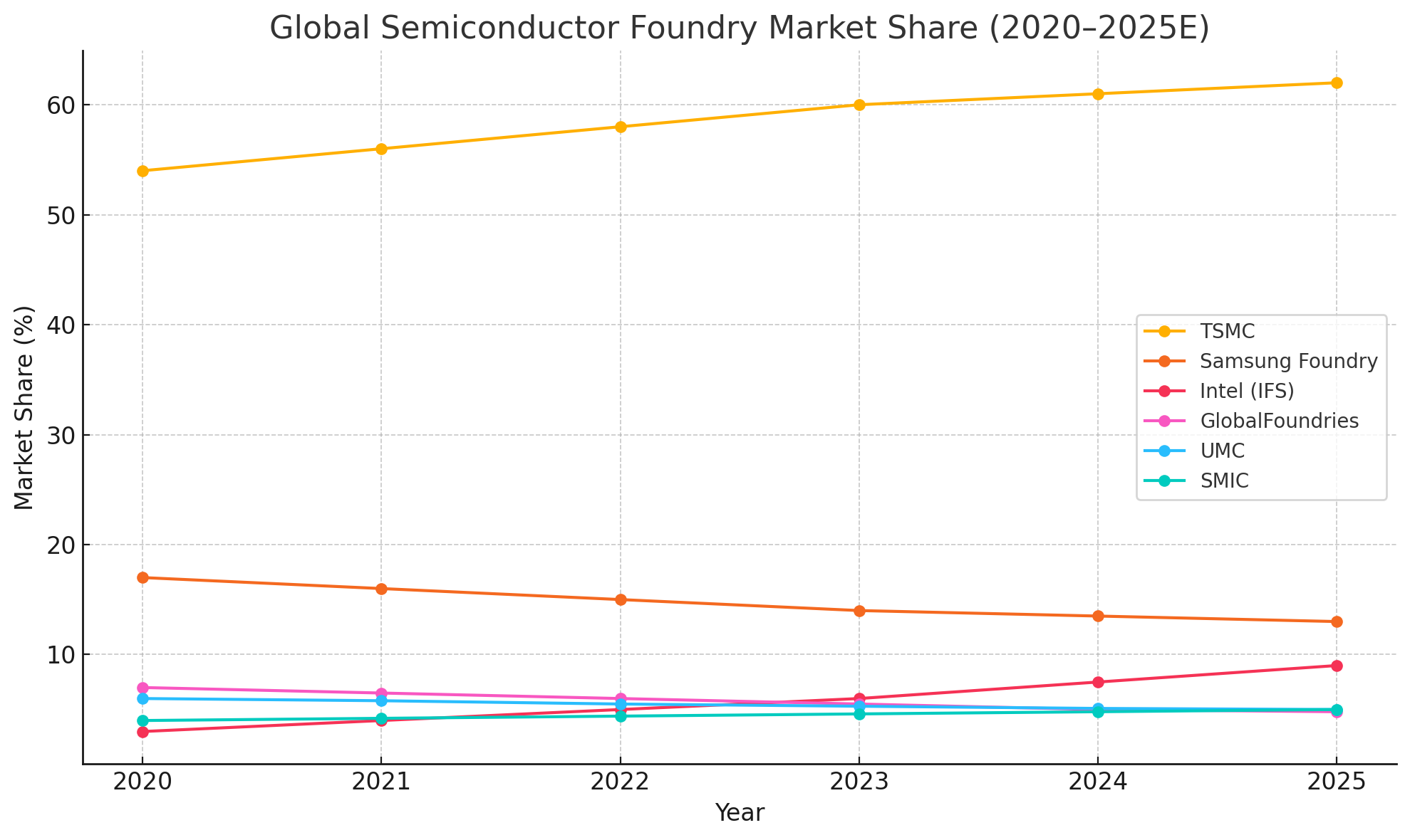
In terms of scale, TSMC has become indispensable to the global economy. As of 2024, it controls over 55% of the global foundry market and manufactures more than 90% of the world’s most advanced chips. Its facilities in Hsinchu, Tainan, and other parts of Taiwan are among the most advanced manufacturing complexes on Earth. The company has also begun expanding internationally, with new fabs under construction in Arizona (U.S.), Kumamoto (Japan), and Dresden (Germany), aiming to address geopolitical concerns and regional diversification mandates.
The Rationale for Collaboration
Despite their different business models and histories, Intel and TSMC now find themselves confronting similar macroeconomic and geopolitical challenges. The semiconductor supply chain is undergoing rapid transformation, driven by surging demand, the need for geographic redundancy, and the growing complexity of chip architectures. Both firms recognize that future success will depend not only on technical excellence but also on strategic alliances that balance autonomy with scalability.
For Intel, aligning with TSMC offers a chance to accelerate its recovery in manufacturing competitiveness. By leveraging TSMC’s mature foundry operations, Intel can offload parts of its production burden, reduce capital expenditures, and gain access to leading-edge process nodes more quickly. This is particularly critical as Intel seeks to compete in AI, GPU, and custom silicon markets that demand rapid time-to-market and high-volume capacity.
For TSMC, the joint venture provides access to Intel’s expansive x86 IP portfolio, advanced packaging technologies, and ecosystem of customers in the enterprise, government, and data center sectors. It also enables TSMC to deepen its footprint in Western markets—especially in the United States, where government incentives are tied to partnerships that enhance domestic production.
Furthermore, both companies face common pressure from China’s semiconductor push and the emergence of new competitors like SMIC, as well as from existing rivals such as Samsung Foundry. A cooperative approach, at least in selective areas of manufacturing, may serve as a bulwark against further fragmentation of the global semiconductor value chain.
Looking Ahead
The convergence of Intel’s foundry ambitions with TSMC’s manufacturing prowess through a formal joint venture signals the beginning of a new chapter. While previous collaborations between the two companies were largely transactional—with Intel outsourcing select chip production to TSMC—this venture marks a strategic shift toward joint innovation, risk sharing, and coordinated execution.
In the subsequent section, we will examine the inner workings of the joint venture itself, including its legal structure, operational blueprint, and shared technological roadmap. Understanding how the alliance is structured will provide further clarity on its potential to succeed—and its limitations.
Inside the Joint Venture: Structure, Goals, and Operations
The establishment of a joint venture between Intel and TSMC marks a profound shift in the semiconductor industry’s collaborative landscape. While previous engagements between the two firms were largely confined to customer-supplier dynamics, this new partnership reflects a deliberate strategy to pursue co-development, mutual scaling, and synchronized innovation. As such, understanding the structural foundation, strategic objectives, and operational mechanisms of the Intel-TSMC joint venture is essential for evaluating its potential efficacy and influence.
Legal and Organizational Structure
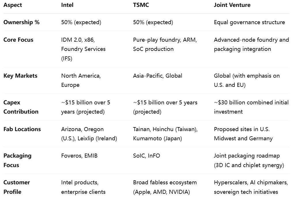
Although exact contractual details have not been made fully public, industry analysts and regulatory disclosures indicate that the joint venture will be structured as an independent legal entity, with shared governance between Intel and TSMC. Both parties are expected to hold substantial equity stakes—likely close to a 50/50 distribution—ensuring balanced decision-making authority and aligned strategic priorities. The board of directors will be composed of representatives from both firms, and leadership appointments are anticipated to reflect the complementary strengths of each organization.
The venture will be incorporated as a limited liability company (LLC) to provide flexibility in operational structuring and to facilitate capital investment from both parent organizations. Key functional areas such as R&D, fab operations, sales, and customer engagement will be integrated within the joint entity, although certain proprietary IP elements are expected to remain segmented and subject to licensing agreements to protect core technologies.
Operational Goals and Technological Mandate
The joint venture’s foremost objective is to enhance global semiconductor manufacturing capacity, particularly in response to escalating demand for high-performance computing (HPC), generative artificial intelligence (AI), 5G infrastructure, and advanced automotive systems. With foundry utilization rates nearing saturation and lead times for advanced process nodes extending across quarters, the need for additional fabrication capability has become urgent.
The new entity will focus on building and operating advanced-node semiconductor fabs, potentially targeting process technologies at or below the 3-nanometer scale. These fabs are likely to be located in strategic geographies including the United States, Europe, and possibly select Asian countries outside of Taiwan and mainland China. The initiative aligns with public policy incentives in key markets—particularly under the U.S. CHIPS Act, which prioritizes domestic semiconductor production for national security and economic resilience.
One of the most significant technological areas of emphasis will be advanced packaging. Intel’s leadership in 3D packaging, specifically its Foveros and EMIB (Embedded Multi-die Interconnect Bridge) technologies, is expected to complement TSMC’s capabilities in chiplet integration and system-on-integrated-chip (SoIC) architectures. The venture is thus positioned not only to produce leading-edge wafers but also to deliver fully integrated semiconductor solutions tailored for next-generation computing workloads.
In addition, the partnership will explore joint development of design enablement tools, process design kits (PDKs), and co-optimization methodologies. These efforts are crucial for enabling fabless semiconductor firms to transition their designs to the new joint platform with minimal rework, thereby broadening the venture’s customer base.
Target Customers and Industry Positioning
Unlike Intel’s traditional IDM focus or TSMC’s broad customer orientation, the joint venture is expected to target a hybrid clientele. This includes not only Intel’s existing hyperscaler and enterprise customers but also select fabless companies operating at the cutting edge of AI, networking, and HPC workloads. Early market signals suggest that the venture may attract design wins from AI hardware startups and sovereign semiconductor programs seeking geopolitical insulation from supply chain risks.
From a market positioning standpoint, the venture will operate as a high-performance foundry, competing with TSMC’s internal operations, Samsung Foundry, and Intel’s standalone IFS business. It will likely offer customized foundry services with differentiated features in packaging, security, and system integration—rather than simply competing on process parity or price.
Geographic Deployment and Supply Chain Strategy
The selection of fabrication locations will be critical to the venture’s geopolitical and logistical strategy. Preliminary reports indicate that the first mega-fab may be constructed in the United States—likely in Ohio or Arizona—where Intel has already established infrastructure and secured federal subsidies. A second site under consideration is Germany, given the European Union’s “Chips Act” initiative and its commitment to revitalizing continental semiconductor capabilities.
These dual-site operations would create regional redundancy and enhance supply chain resilience, allowing the venture to serve customers in North America and Europe more directly while mitigating geopolitical risks associated with East Asia. This distributed model also aligns with growing industry interest in "fab clustering," which seeks to co-locate supply chain partners to minimize transit costs and reduce exposure to natural or political disruptions.
Furthermore, the joint venture is expected to implement a vertically coordinated supply chain strategy, integrating upstream and downstream partners—including substrate suppliers, EDA tool providers, and assembly/test service vendors—into a cohesive operational framework.
Challenges and Strategic Risk Factors
Despite the compelling rationale behind the joint venture, several risks remain. Cultural differences between Intel and TSMC may complicate integration efforts, particularly in areas of operational governance and IP sharing. Intel’s historic emphasis on proprietary systems may contrast with TSMC’s customer-centric openness, potentially creating friction in roadmap alignment.
Additionally, regulatory scrutiny—especially from antitrust authorities in the U.S., Europe, and Asia—may delay or condition the venture’s approval. Governments are likely to assess whether the venture limits competition, particularly if it consolidates access to advanced-node manufacturing capacity among a small group of global players.
Finally, the long payback period associated with semiconductor capital investments could strain balance sheets if demand forecasts prove overly optimistic or if macroeconomic conditions deteriorate.
Strategic Implications for the Semiconductor Ecosystem
The formation of a joint venture between Intel and TSMC is not merely a bilateral business transaction—it is a transformational event with far-reaching implications across the global semiconductor ecosystem. From altering competitive dynamics to influencing government policy and reshaping customer expectations, the reverberations of this alliance are poised to reshape the architecture of global chip manufacturing. In this section, we examine the strategic impact of the Intel-TSMC collaboration across four primary domains: industry competitors, customer relationships, geopolitical considerations, and supply chain realignment.
Impact on Competitors: A New Axis of Power
Perhaps the most immediate consequence of the joint venture is the strategic pressure it exerts on other semiconductor foundries, most notably Samsung Foundry, GlobalFoundries, United Microelectronics Corporation (UMC), and China’s Semiconductor Manufacturing International Corporation (SMIC).
Samsung Foundry, which has positioned itself as the principal challenger to TSMC in advanced-node production, now faces an intensified competitive landscape. While Samsung benefits from vertical integration and access to cutting-edge EUV lithography, the combined force of Intel and TSMC may outmatch it in both process node innovation and packaging capabilities. Moreover, if the joint venture succeeds in establishing a geographically diversified footprint in the United States and Europe, Samsung could lose critical strategic leverage in negotiations with Western customers and governments.
GlobalFoundries and UMC, which specialize in mature nodes and specialty processes, may not be directly impacted by the high-end technical focus of the joint venture. However, as the new alliance scales, it may drive down costs and accelerate time-to-market for advanced technologies—pressuring mid-tier foundries to invest more heavily in innovation or risk marginalization.
SMIC, operating under U.S. trade restrictions, may interpret the joint venture as a geopolitical maneuver designed to isolate China from advanced semiconductor capabilities. The U.S. and its allies have already imposed strict controls on the export of EUV tools to China, and the joint venture could further cement a technology bifurcation between the West and the East, limiting SMIC’s access to critical markets and intellectual property.
Customer Dynamics: New Opportunities and Dilemmas
From a customer standpoint, the Intel-TSMC partnership introduces both opportunity and uncertainty. For Intel’s existing clients, especially enterprise, data center, and defense customers, the venture promises increased manufacturing capacity, technological customization, and geographic proximity—factors that are increasingly valued in procurement decisions.
Fabless companies, which rely heavily on TSMC’s foundry services, may face a strategic dilemma. On one hand, they could benefit from improved production lead times and access to cutting-edge packaging technologies. On the other hand, some may express concern about potential conflicts of interest, particularly if their designs are being fabricated in a facility jointly operated by Intel—a competitor in many segments of the silicon landscape. To mitigate these concerns, the joint venture must enforce strict operational firewalls and establish trust through transparent service-level agreements.
Hyperscalers and AI startups—entities that demand custom silicon and massive compute power—stand to gain the most. These customers will be drawn to the venture’s ability to offer vertically integrated solutions at the frontier of performance and efficiency. By unifying Intel’s IP portfolio with TSMC’s fabrication prowess, the joint venture is uniquely positioned to serve emerging use cases in generative AI, autonomous systems, and large-scale analytics.
Government and Geopolitical Implications
The geopolitical dimension of the Intel-TSMC joint venture cannot be overstated. Amid growing concerns about semiconductor supply chain security, the collaboration serves as a powerful symbol of allied industrial cooperation. Both the U.S. and European Union have expressed strategic interest in bolstering domestic semiconductor production, and the joint venture aligns well with legislative priorities such as the U.S. CHIPS and Science Act and the EU Chips Act.
In the United States, the joint venture could become a flagship project for public-private collaboration, especially if it qualifies for federal funding and tax incentives. Its ability to create jobs, stimulate local economies, and reduce dependence on overseas fabs will be seen as a geopolitical win. Furthermore, by anchoring advanced manufacturing on U.S. soil, the venture enhances national security by ensuring that critical defense and aerospace components can be produced domestically.
In Taiwan, the venture represents both an opportunity and a strategic gamble. While it extends TSMC’s influence globally, it also introduces the risk of intellectual property dispersion and talent migration, particularly if advanced R&D and production capabilities shift to the U.S. or Europe. Taiwanese policymakers will closely monitor the venture’s evolution to ensure that it does not erode the island’s centrality in the global chip supply chain.
Meanwhile, in China, the joint venture will likely be perceived as a further escalation of the West’s efforts to restrict its access to advanced semiconductor technologies. The Chinese government may respond by accelerating investments in indigenous chip manufacturing, redoubling efforts to subsidize national champions, or even imposing countermeasures to protect its technology sovereignty.
Supply Chain Realignment and Ecosystem Effects
The operational strategy of the Intel-TSMC venture will necessitate a realignment of global semiconductor supply chains. With fabs potentially located in Ohio and Germany, the venture will need to establish robust regional supplier networks—including wafer material providers, tool manufacturers, packaging specialists, and logistics partners. This could catalyze the development of fab clusters or semiconductor hubs in these regions, much like those found in Taiwan and South Korea.
Moreover, the venture’s emphasis on 3D packaging, chiplet architectures, and heterogeneous integration will have downstream effects on EDA tool developers, substrate vendors, and OSAT (Outsourced Semiconductor Assembly and Test) firms. Companies like Cadence, Synopsys, ASE Group, and Amkor Technology will need to adapt their offerings to support increasingly complex designs that blur the boundaries between chip, package, and system.
There may also be a cascading effect on workforce development. As the venture expands its operations, it will create demand for highly skilled engineers, material scientists, and operations specialists. Governments may respond with targeted education initiatives and talent attraction programs to support semiconductor workforce growth, further integrating the public and private sectors.
Financial and Technological Impact
Rethinking Scale and Innovation
The Intel-TSMC joint venture represents not only a strategic realignment but also a significant financial and technological undertaking. With an estimated initial investment exceeding $30 billion, the venture underscores the capital intensity of advanced semiconductor manufacturing and the high stakes involved in maintaining global leadership in chip innovation. Beyond the sheer scale of capital expenditures, the partnership signals a forward-looking redefinition of how semiconductor firms approach process technology, packaging integration, and system-level optimization. This section assesses the financial structure, cost-benefit considerations, innovation roadmap, and broader industry ramifications of the joint venture.
Capital Expenditure and Funding Strategy
Semiconductor fabrication at advanced nodes—particularly 3nm and below—requires monumental financial commitment. According to industry estimates, a single cutting-edge fab capable of supporting 2nm production can cost upwards of $15–20 billion. The joint venture between Intel and TSMC is expected to include at least two such fabs, with one located in the United States and another potentially in Europe. Combined capital expenditures for these facilities, along with associated R&D centers, packaging labs, and workforce development initiatives, are projected to exceed $30 billion over the next five to seven years.
The funding model will likely involve a mix of equity contributions from both parent firms, public-private partnerships, and government incentives. In the U.S., the venture is poised to benefit from the CHIPS and Science Act, which allocates more than $52 billion in federal subsidies and research grants to support domestic semiconductor initiatives. State-level tax credits and infrastructure support—particularly in Ohio and Arizona—will also help defray capital costs. In Europe, the venture could tap into resources from the EU Chips Act, which seeks to double the continent’s share of global semiconductor production by 2030.
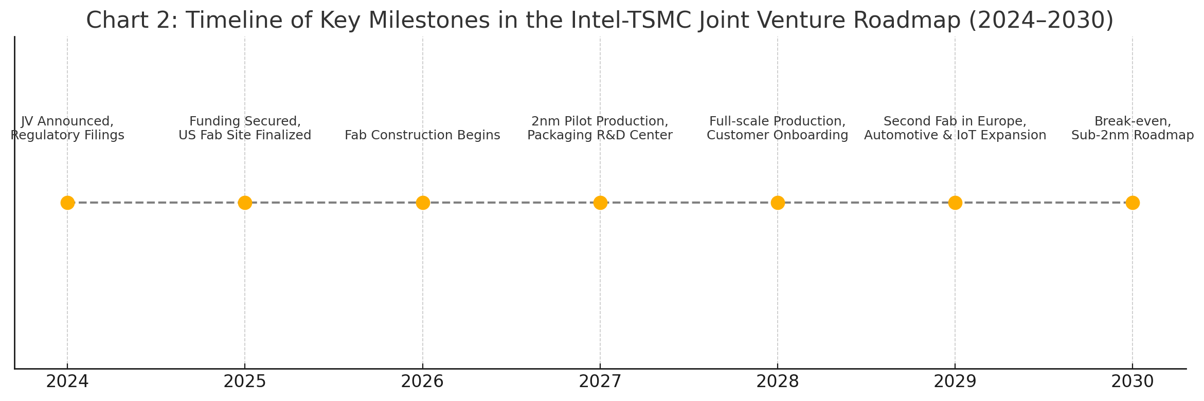
Financial analysts anticipate that the joint venture will operate under a balanced capital structure, with both Intel and TSMC maintaining equal or near-equal ownership to ensure aligned governance. Initial returns may be modest given the long gestation period typical of semiconductor projects, but the venture is expected to reach operational breakeven by 2029 or 2030, driven by volume production, customer onboarding, and yield optimization.
Revenue Potential and Market Positioning
The revenue model for the joint venture will be distinct from either parent company’s traditional structure. Unlike Intel’s internal fabrication for proprietary products, or TSMC’s wide-scale outsourcing model, the new entity will function as a hybrid specialized foundry, focusing on high-margin, performance-critical applications. These include AI accelerators, next-generation CPUs, 5G baseband processors, automotive SoCs, and custom chips for hyperscale data centers.
The joint venture is also expected to implement a value-added pricing model, leveraging its unique capabilities in 3D integration, chiplet architecture, and co-packaged optics. While this may limit its competitiveness in commoditized segments, it positions the venture favorably in premium markets where design differentiation and energy efficiency are paramount.
Projections from semiconductor market research firms suggest that the venture could generate annual revenues of $8–10 billion within five years of full production, with EBITDA margins exceeding 25% once economies of scale and high-volume production are achieved. This would place the venture in direct competition with leading-edge divisions of Samsung Foundry and TSMC’s own internal operations, though it would remain smaller in overall volume compared to TSMC’s mainstream foundry business.
Innovation Trajectory: Process Nodes and Packaging Technologies
Technologically, the joint venture is uniquely positioned to push the envelope in both process technology and advanced packaging. While TSMC brings unmatched expertise in wafer fabrication, Intel contributes pioneering work in 3D packaging and system integration. This complementary innovation portfolio offers an opportunity to transcend traditional scaling limitations defined by Moore’s Law.
In terms of process technology, the venture is expected to begin production on a customized variant of TSMC’s N2 (2nm-class) node, incorporating process optimizations tailored for Intel’s x86 architecture and new AI workloads. By 2028 or 2029, the roadmap is expected to evolve toward sub-2nm nodes—possibly leveraging gate-all-around (GAA) transistor architectures and backside power delivery networks, technologies that promise significant performance and power efficiency gains.
Equally transformative is the venture’s emphasis on packaging innovation. Intel’s Foveros and EMIB technologies, combined with TSMC’s SoIC and CoWoS platforms, enable heterogeneous integration—allowing different functional blocks (CPU, GPU, memory, AI cores) to be packaged together in a single module with ultra-high bandwidth and minimal latency. These packaging techniques reduce interconnect power loss and open new avenues for customized chip design, particularly in AI inference and edge computing scenarios.
Furthermore, the joint venture is expected to establish a dedicated design enablement and packaging co-optimization center, where customers can work with the engineering teams to fine-tune architectural layouts for specific performance goals. This will include the co-development of design kits, simulation tools, and thermal management models to reduce time-to-market and improve reliability.
Strategic Differentiation and Long-Term Technological Impact
The most significant technological impact of the joint venture may lie in its ability to redefine design and manufacturing convergence. As chip complexity increases and traditional node scaling slows, performance improvements will increasingly depend on vertical integration across design, fabrication, and packaging. The joint venture’s ability to offer system-level optimization, rather than just wafer-level services, represents a new paradigm in semiconductor value creation.
Moreover, the venture is well-positioned to act as a testbed for future innovations, including AI-assisted design automation, quantum chip packaging, and photonic-electronic integration. With dedicated R&D funding from both parent companies and strong academic collaborations expected in the U.S. and Europe, the joint venture could serve as a nucleus for the next wave of semiconductor breakthroughs.
This innovation potential also enhances the venture’s appeal to sovereign technology initiatives. Governments looking to secure domestic access to advanced semiconductor technologies may favor the joint venture for strategic contracts, especially if it can demonstrate leadership in both performance and reliability. In this context, the venture not only becomes a business entity but also a platform for industrial policy execution.
Risks and Financial Contingencies
Despite its promise, the joint venture faces several financial and technological risks. On the financial side, cost overruns, delays in fab construction, or slower-than-expected customer ramp could strain cash flows and push breakeven timelines further into the future. Geopolitical tensions or shifts in regulatory regimes could also disrupt supply chain continuity and market access.
Technologically, integration challenges may arise from differences in manufacturing philosophies, tool chains, and quality assurance practices between Intel and TSMC. These differences must be reconciled through robust joint operating procedures and cross-company engineering coordination.
Additionally, the venture must guard against technological obsolescence. With competitors such as Samsung, AMD, and NVIDIA pursuing aggressive innovation strategies, the joint venture will need to continuously reinvest in R&D to stay at the cutting edge of process and packaging technologies.
A New Era for the Global Foundry Market
The announcement of a joint venture between Intel and TSMC marks a defining moment in the ongoing evolution of the semiconductor industry. It signals a profound transformation in how global chipmakers approach capacity expansion, technological collaboration, and strategic positioning in an increasingly volatile geopolitical environment. Through this partnership, two of the world’s most influential semiconductor companies are forging a new path—one that could recalibrate competitive dynamics, influence industrial policy, and lay the groundwork for the next decade of computing innovation.
At its core, the Intel-TSMC joint venture is a strategic response to a converging set of challenges and opportunities. On one hand, the industry is grappling with supply chain vulnerabilities, soaring capital expenditures, and a relentless demand for ever-more-powerful and energy-efficient chips. On the other hand, there is a window of opportunity to reimagine traditional roles, share risk, and combine strengths in ways that were previously considered unlikely or even untenable.
From Intel’s perspective, the joint venture reinforces its IDM 2.0 strategy, which acknowledges the limitations of vertical integration in a world of accelerating specialization. By collaborating with TSMC—an organization globally recognized for manufacturing excellence—Intel gains access to best-in-class process technologies, which are essential for remaining competitive in artificial intelligence, high-performance computing, and custom silicon. The partnership also allows Intel to scale its manufacturing ambitions more efficiently, particularly in geographies that align with U.S. industrial policy.
For TSMC, the alliance represents a nuanced evolution of its foundry model. While historically operating as a neutral, customer-first fabrication partner, TSMC now enters a more strategic form of co-development with a former competitor. This move enables the company to expand its footprint outside of Taiwan, diversify its geopolitical exposure, and deepen relationships with Western customers and governments. It also allows TSMC to tap into Intel’s decades-long expertise in chip architecture, packaging, and enterprise-grade systems engineering.
The structure of the joint venture—likely featuring equal equity contributions, shared governance, and regionally distributed fabs—illustrates a broader industry trend toward hybrid operating models. These models blend internal IP development with external manufacturing partnerships, and increasingly rely on co-packaged systems, chiplet integration, and design enablement platforms. The Intel-TSMC alliance thus becomes a template for future public-private and cross-border collaborations in high-tech manufacturing.
As detailed in earlier sections, the venture’s operational roadmap is both ambitious and methodically staged. It begins with site selection and initial construction in the United States and Europe, progresses through pilot production and advanced packaging development, and culminates in full-scale commercialization across multiple end markets. The projected timeline suggests the venture will reach breakeven by the end of this decade, contingent upon smooth ramp-up, yield optimization, and customer onboarding.
Yet the strategic implications of this partnership extend well beyond financial metrics. In the context of growing technological nationalism and the weaponization of supply chains, the Intel-TSMC joint venture may serve as a geopolitical stabilizer. By reinforcing trusted supply networks between the U.S., Taiwan, and the European Union, the venture contributes to a more secure and resilient semiconductor ecosystem—less dependent on single points of failure and more aligned with democratic values and open innovation.
At the same time, this collaboration could prompt competitive reactions from other global players. Samsung Foundry may accelerate its U.S. expansion and intensify its R&D efforts. China, perceiving this alliance as an exclusionary bloc, may redouble investments in domestic fabrication capabilities and seek alternative trade alliances. Foundries such as GlobalFoundries, UMC, and SMIC will need to reassess their market positioning and innovation priorities to remain relevant.
For customers, the joint venture introduces both enhanced capabilities and new considerations. High-performance computing firms, AI startups, and hyperscalers will benefit from access to a manufacturing partner that combines cutting-edge process nodes with customizable packaging solutions. However, customers will also need reassurances about intellectual property protection, supply chain neutrality, and the competitive boundaries between the joint venture and the parent companies’ core businesses.
Policymakers and regulators, meanwhile, must navigate a delicate balance. On one hand, the venture aligns with stated objectives to strengthen domestic semiconductor production and reduce reliance on foreign suppliers. On the other hand, regulatory bodies must ensure that such collaborations do not result in anti-competitive behavior, undue concentration of technological power, or the erosion of open market principles. Clear guidelines, robust compliance mechanisms, and international coordination will be essential to ensuring the joint venture serves the public interest.
From a technological standpoint, the joint venture presents an extraordinary opportunity to reimagine the future of chip manufacturing. The convergence of Intel’s packaging leadership and TSMC’s process mastery opens the door to innovations that could redefine performance benchmarks across industries. Whether in AI model training, edge computing, autonomous systems, or space technology, the output of this collaboration could power breakthroughs that were previously out of reach due to constraints in scale, energy efficiency, or system integration.
Nevertheless, the path ahead is not without risks. Operational misalignment, cultural differences, regulatory hurdles, and market volatility all pose challenges to the venture’s success. Failure to deliver on promised milestones could not only affect shareholder value but also undermine confidence in large-scale industrial collaborations more broadly. Therefore, sustained executive alignment, agile governance, and transparent communication will be essential to managing expectations and maintaining strategic focus.
As we look to the decade ahead, the Intel-TSMC joint venture may come to symbolize the dawn of a new era in the global foundry market—one defined not by unilateral dominance but by strategic interdependence. In this era, partnerships will serve as the primary engine of progress, blending specialization with scale, and innovation with resilience. The success of the joint venture could serve as a model for how industry leaders can collaboratively solve systemic challenges, navigate geopolitical complexity, and deliver on the promise of the digital age.
In conclusion, while the future remains uncertain, the Intel-TSMC joint venture represents a bold and timely response to the most pressing issues facing the semiconductor industry today. It reflects a recognition that in an era of global interconnectivity, the most effective way forward may not be to go it alone, but to move forward—together.
References
- Intel Unveils IDM 2.0 Strategy to Drive Manufacturing Innovation
https://www.intel.com/content/www/us/en/newsroom/news/idm-2-0-manufacturing-innovation.html - TSMC Corporate Overview and Foundry Business Model
https://www.tsmc.com/english/aboutTSMC/company_profile.htm - U.S. CHIPS and Science Act Summary and Incentives
https://www.commerce.gov/chips - EU Chips Act: Strengthening Europe’s Semiconductor Capabilities
https://digital-strategy.ec.europa.eu/en/policies/eu-chips-act - Intel Foundry Services: Advancing the Global Foundry Ecosystem
https://www.intel.com/content/www/us/en/foundry/overview.html - TSMC Technology Roadmap and Advanced Node Development
https://www.tsmc.com/english/dedicatedFoundry/technology - Samsung Foundry Overview and Competitive Landscape
https://semiconductor.samsung.com/us/foundry/ - GlobalFoundries Capabilities and U.S. Expansion Initiatives
https://gf.com/about - Semiconductor Market Trends and Advanced Packaging Innovations
https://www.semiconductors.org/market-data/ - SMIC Corporate Strategy and China’s Semiconductor Push
https://www.smics.com/