
China Develops World's Fastest Transistor Using Light and Sound Waves: A Leap in Photonic-Acoustic Computing

In an era defined by rapid technological evolution and fierce global competition, the semiconductor industry stands at the heart of geopolitical tensions, scientific ambition, and economic growth. For decades, transistor scaling, encapsulated by Moore’s Law, has served as the foundational principle guiding the pace of progress in computing. Yet, as silicon-based technologies approach their physical and thermodynamic limits, nations and corporations are intensifying their search for breakthrough alternatives. In this context, China’s recent announcement of having developed the world’s fastest transistor—powered by a novel combination of light and sound waves—marks a potentially historic leap in the future of computing.
This innovation, led by a team of Chinese scientists, introduces a radical departure from conventional electronic transistor mechanisms. Rather than relying solely on the movement of electrons through silicon substrates, the newly unveiled transistor leverages the interaction between photons and phonons—light and sound waves, respectively—to process and switch signals at unprecedented speeds. According to early data, this hybrid photonic-acoustic transistor surpasses all current benchmarks for switching frequency, speed, and energy efficiency, setting the stage for a new class of ultrafast, low-power computing devices.
The strategic importance of this development cannot be overstated. Transistors are the elemental building blocks of all modern electronics—from smartphones and data centers to quantum processors and artificial intelligence (AI) accelerators. The ability to manipulate information faster and more efficiently than current technologies allows for vast improvements in computing performance, energy consumption, and miniaturization. These gains, in turn, unlock new capabilities in fields as diverse as real-time AI inference, high-frequency trading, secure communications, and next-generation scientific research.
China's achievement is not only a scientific milestone but also a geopolitical signal. In recent years, the United States and its allies have imposed stringent export controls on advanced chipmaking tools and semiconductor technologies to curb China’s technological ascent. These restrictions have affected China's access to cutting-edge fabrication equipment and intellectual property, leading the country to aggressively invest in homegrown alternatives. By developing a transistor that may ultimately sidestep the need for traditional CMOS-based lithographic manufacturing, China is asserting itself as a credible leader in post-silicon computing innovation.
Beyond its scientific novelty, the transistor’s architecture speaks volumes about the emerging trends in materials science and nanotechnology. Utilizing advanced substrates like gallium arsenide and lithium niobate, the design demonstrates how quantum-scale interactions can be engineered to transmit and convert energy more efficiently than through electrons alone. In essence, by harnessing the wave-like properties of both light and sound, the transistor moves beyond binary logic gates into a realm where multiple forms of energy can be orchestrated to perform computational tasks simultaneously. This multiphysics paradigm has the potential to dramatically increase transistor throughput and reduce heat dissipation—two of the most critical bottlenecks in today’s semiconductor design.
The international research community has long speculated about the possibilities of integrating photonics and phononics into future transistors, but practical implementations have been elusive. High-precision alignment, optical loss, and compatibility with existing semiconductor fabrication processes have been major obstacles. China’s breakthrough suggests that some of these barriers have now been partially, if not fully, overcome. While independent verification of performance metrics remains pending, the sheer ambition of the project and its reported results warrant serious attention from both the academic and commercial sectors.
Moreover, this development comes at a time when alternative transistor technologies—such as those based on graphene, carbon nanotubes, and 2D materials—are also making headlines. However, many of these approaches are still years away from practical deployment due to their inherent scalability and manufacturability issues. In contrast, a photonic-acoustic transistor that integrates with or enhances existing silicon ecosystems may offer a faster path to commercialization. The potential for hybrid integration, wherein traditional chips are augmented with light-sound switching cores, opens up intriguing possibilities for interim adoption while full photonic-acoustic architectures mature.
As nations increasingly define technological leadership in terms of semiconductor autonomy and innovation, breakthroughs such as China’s light-sound transistor may redefine global power dynamics. With its focus on achieving self-sufficiency in advanced computing infrastructure, China has aligned this innovation with broader policy initiatives such as “Made in China 2025” and the “14th Five-Year Plan for Science and Technology.” If the technology proves viable at scale, it could catalyze a wave of new research, industrial investment, and international partnerships—or conversely, intensify the techno-nationalist fragmentation already reshaping global supply chains.
In the sections that follow, we will explore the core scientific principles that enable this revolutionary transistor, analyze its potential impact on the global semiconductor landscape, examine its real-world applications, and address the challenges that must be overcome before the technology can be deployed at scale. We will also present comparative data through charts and tables to contextualize the innovation against current transistor technologies.
This is more than a marginal improvement or laboratory curiosity—it may represent a paradigm shift in the design and function of computational systems. As the world moves toward ever-increasing data demands, edge computing, and AI ubiquity, technologies capable of delivering faster, leaner, and more intelligent processing will be indispensable. Whether this new transistor marks the beginning of a post-silicon era or merely a significant evolutionary branch of existing research, one thing is clear: China has signaled its intent to lead the next frontier of semiconductor innovation—and the world is paying attention.
The Science Behind the Breakthrough
The development of the world’s fastest transistor, employing a synergistic interaction of light and sound waves, marks a significant scientific milestone with implications extending far beyond conventional electronics. To understand the gravity of this innovation, one must delve into the fundamental science that underpins the operation of this hybrid device. At its core, the transistor exploits the physical interplay between photons (light particles) and phonons (quantized sound vibrations) to achieve data switching at speeds that far surpass those of traditional semiconductor devices. This section offers a comprehensive exploration of the underlying principles, materials, architecture, and comparative performance of this new class of transistor.
Fundamental Mechanisms: Photonic-Phononic Interplay
Traditional transistors rely on the control of electron flow through a semiconductor material such as silicon. The switching speed of these devices is limited by factors such as carrier mobility, parasitic capacitance, and thermal dissipation. In contrast, the photonic-acoustic transistor replaces or augments electrical signals with energy waves—specifically photons and phonons—opening the door to fundamentally faster and more efficient switching mechanisms.
Photons, the elementary particles of light, travel at the highest speed permitted by the laws of physics and do not suffer from resistive heating, a major limitation in electronic transistors. Phonons, on the other hand, represent vibrational energy in the crystal lattice of a material and are known to mediate interactions in optomechanical and acousto-optic systems. The key innovation here lies in coupling these two forms of energy to trigger and modulate the transistor's switching state.
This coupling is achieved through the acousto-optic effect, a phenomenon where the refractive index of a material changes in response to mechanical vibrations. This change alters how light propagates through the medium. When a sound wave—generated through piezoelectric or electromechanical means—travels through a waveguide, it modulates the optical path length or direction of the incident light beam. The resulting dynamic control over light enables the device to switch between binary states at speeds limited only by the propagation of light and sound within nanoscale structures.
Materials and Fabrication
The selection of materials is paramount to achieving such high switching speeds. While silicon has been the mainstay of semiconductor devices for decades, it has well-known limitations in photonic applications due to its indirect bandgap and limited optical transparency in certain wavelength regimes. To circumvent these issues, the Chinese research team utilized gallium arsenide (GaAs) and lithium niobate (LiNbO₃)—two materials with exceptional electro-optic and acousto-optic properties.
Gallium arsenide offers superior electron mobility compared to silicon and supports efficient photonic integration. Its direct bandgap allows for better photon emission and absorption, making it suitable for optoelectronic devices. Lithium niobate, on the other hand, is a ferroelectric crystal that exhibits strong piezoelectric and electro-optic behavior, making it ideal for acoustic wave generation and light modulation. These materials were integrated using advanced heterogeneous integration techniques, combining different substrates at the nanoscale without compromising structural integrity or signal coherence.
Advanced electron-beam lithography, nanoimprint lithography, and molecular beam epitaxy (MBE) were employed to fabricate the intricate nanostructures required for precise control of light and sound pathways. The manufacturing process also involved the creation of ultra-thin waveguides, phononic resonators, and optical cavities to localize and manipulate energy with minimal loss.
Architecture and Operational Principles
The architecture of the photonic-acoustic transistor is a departure from conventional metal-oxide-semiconductor field-effect transistor (MOSFET) design. Instead of relying on a gate to modulate electron flow between the source and drain terminals, the hybrid device includes:
- A phononic actuator to generate surface acoustic waves (SAWs),
- An optical waveguide or resonator to direct photons,
- An interaction region where phonon-induced refractive index modulation alters the path or phase of light, and
- An output coupler to detect the light's altered state, translating it back into digital information.
In operation, a phononic pulse propagates through the interaction region and temporarily changes the refractive index of the waveguide. When a laser or light pulse is concurrently sent through the waveguide, this modulation redirects or alters the light signal, effectively switching its path or state. By carefully timing these interactions, logic operations and signal routing can be performed at frequencies exceeding terahertz (THz) ranges.
Early experimental results demonstrate switching times in the sub-femtosecond range (i.e., less than one quadrillionth of a second), an order of magnitude faster than current CMOS or even emerging graphene-based devices. Additionally, the energy required per switching operation is markedly lower, owing to the lack of resistive heating and capacitive charging.
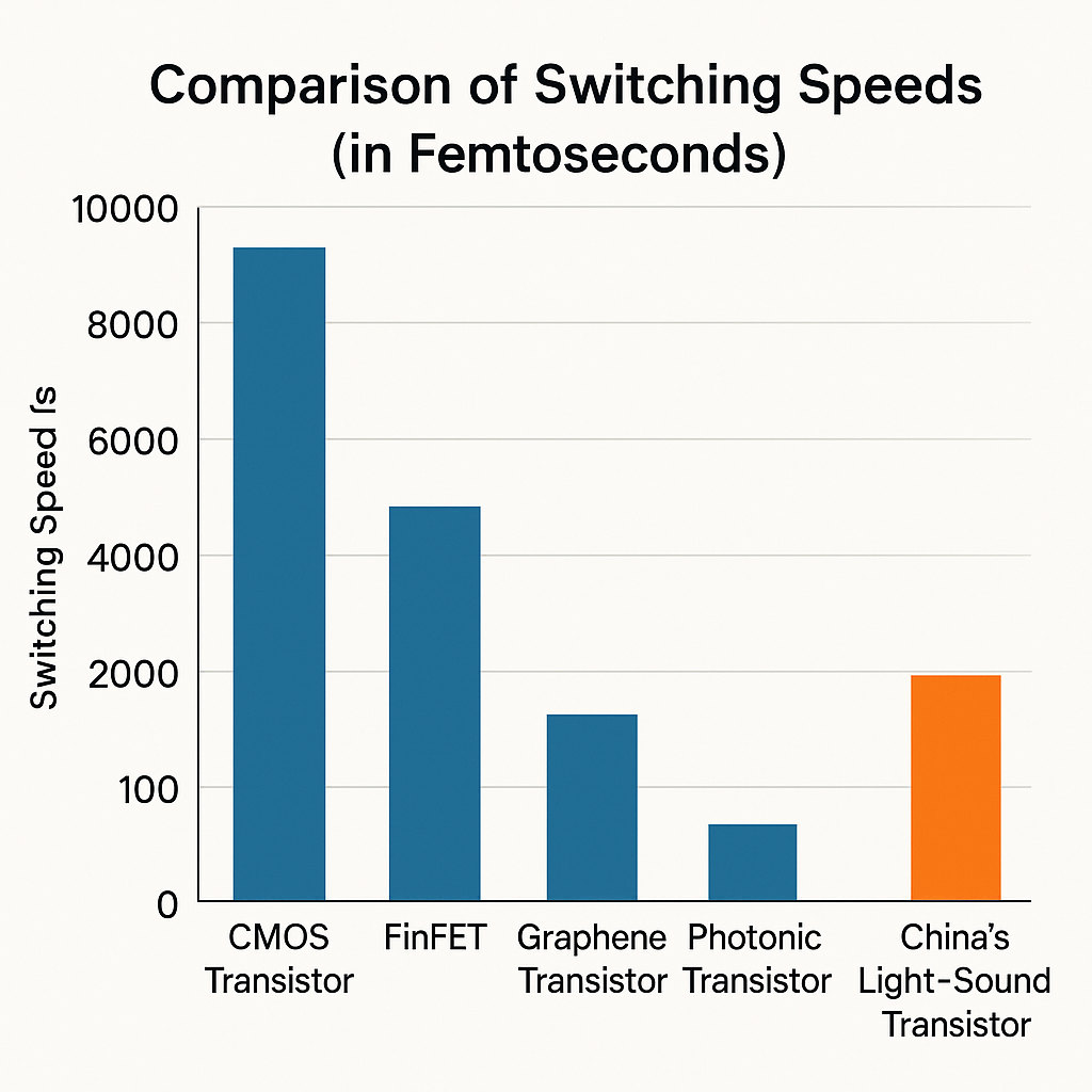
This comparison underscores the enormous potential of the hybrid device in applications where speed is paramount.
Integration Potential and Scalability
A key question surrounding any novel transistor design is its compatibility with existing semiconductor ecosystems. The Chinese-developed device, while based on unconventional principles, is designed with integration in mind. The use of III-V semiconductors and optical elements allows for potential co-packaging with silicon chips using photonic interposers. This architecture is conducive to chiplet-based design, wherein optical, acoustic, and electronic components can coexist on the same substrate or be connected through ultra-fast optical interconnects.
The scalability of this design is contingent upon advances in nanofabrication techniques, particularly in ensuring uniformity and alignment across millions or billions of devices per wafer. Preliminary reports suggest that the design is modular, allowing individual units to be replicated with minor variations in input/output coupling to accommodate different logic functions. Moreover, the reduced thermal load associated with non-electronic switching enables higher density packing of components without the need for aggressive cooling solutions.
Comparative Edge Over Emerging Technologies
The photonic-acoustic transistor exists at the convergence of several promising research paths, including photonics, phononics, quantum computing, and neuromorphic architectures. Unlike purely photonic transistors, which struggle with deterministic switching and compact size, or graphene devices that remain difficult to fabricate at scale, this hybrid transistor leverages well-understood material interactions and mature optical principles.
Additionally, the hybrid nature of the device could be adapted to support multi-state logic, thereby breaking the binary limitations of traditional logic gates. This would enable new classes of computation that mimic neural behavior or quantum superposition, providing a route to brain-inspired computing models.
In summary, the scientific underpinnings of China’s photonic-acoustic transistor are grounded in the careful orchestration of light and sound at the nanoscale, utilizing advanced materials and innovative fabrication strategies. The approach offers significant performance advantages over both traditional and emerging transistor technologies in terms of speed, efficiency, and integration potential. As the global tech ecosystem prepares for a post-silicon era, this breakthrough demonstrates that manipulating multiple physical domains concurrently may be key to unlocking the next generation of high-performance computing.
Strategic Implications for the Semiconductor Industry
The unveiling of China’s photonic-acoustic transistor, heralded as the fastest in the world, extends far beyond scientific novelty. It carries with it a profound set of strategic implications for the global semiconductor industry. As transistors remain the bedrock of all digital infrastructure—powering everything from smartphones and data centers to artificial intelligence and defense systems—any meaningful advancement in their design and performance reverberates through global supply chains, trade policies, and technological hierarchies. This section explores how China's latest transistor innovation could reshape industry dynamics, alter competitive balances, and challenge the current technological hegemony.
Reinforcing China's Strategic Semiconductor Ambitions
China has long aspired to reduce its reliance on foreign semiconductor technologies. Faced with escalating export controls, including the United States’ restrictions on advanced lithography tools and AI chip architectures, Beijing has responded by investing heavily in domestic research and development. The country’s flagship policy initiatives—including the “Made in China 2025” plan and the 14th Five-Year Plan—explicitly prioritize semiconductor self-sufficiency and frontier innovation.
The development of a light-sound transistor aligns squarely with these goals. Unlike traditional CMOS-based devices that depend on extreme ultraviolet (EUV) lithography—a field dominated by ASML of the Netherlands—photonic-acoustic transistors potentially sidestep this bottleneck. By leveraging alternative materials and wave-based energy transfer, this breakthrough may allow China to chart an independent path forward, unencumbered by Western toolchains and proprietary standards.
Such a move is not merely technological; it is deeply geopolitical. The ability to manufacture ultra-fast transistors domestically represents a leap in China’s quest for technological sovereignty, granting the nation not only a commercial edge but also a form of digital autonomy that has significant implications for cyber-defense, national security, and industrial policy.
Disruption of the Global Semiconductor Value Chain
The global semiconductor industry is intricately interconnected, with design, manufacturing, and packaging spread across different continents. Innovations that deviate from the dominant silicon-based architecture risk disrupting these tightly coupled ecosystems. The light-sound transistor, if proven viable at scale, could undermine the existing value chain in several ways.
First, incumbent leaders—such as Intel, TSMC, and Samsung—have made enormous investments in next-generation silicon processes, including 2nm and sub-2nm nodes. A viable alternative technology that performs exponentially better and does not rely on lithographic miniaturization could devalue these investments. Second, firms specializing in electronic design automation (EDA) tools may need to pivot to support new design paradigms that incorporate photonic and phononic simulation models, a transition that requires significant tooling and intellectual property redevelopment.
Third, the shift toward hybrid transistor technologies could favor companies with vertical integration across materials science, optics, and quantum computing, rather than firms that have excelled solely in electronic circuit design. This reorientation may create opportunities for emergent players while putting pressure on legacy firms to reinvent their R&D roadmaps.
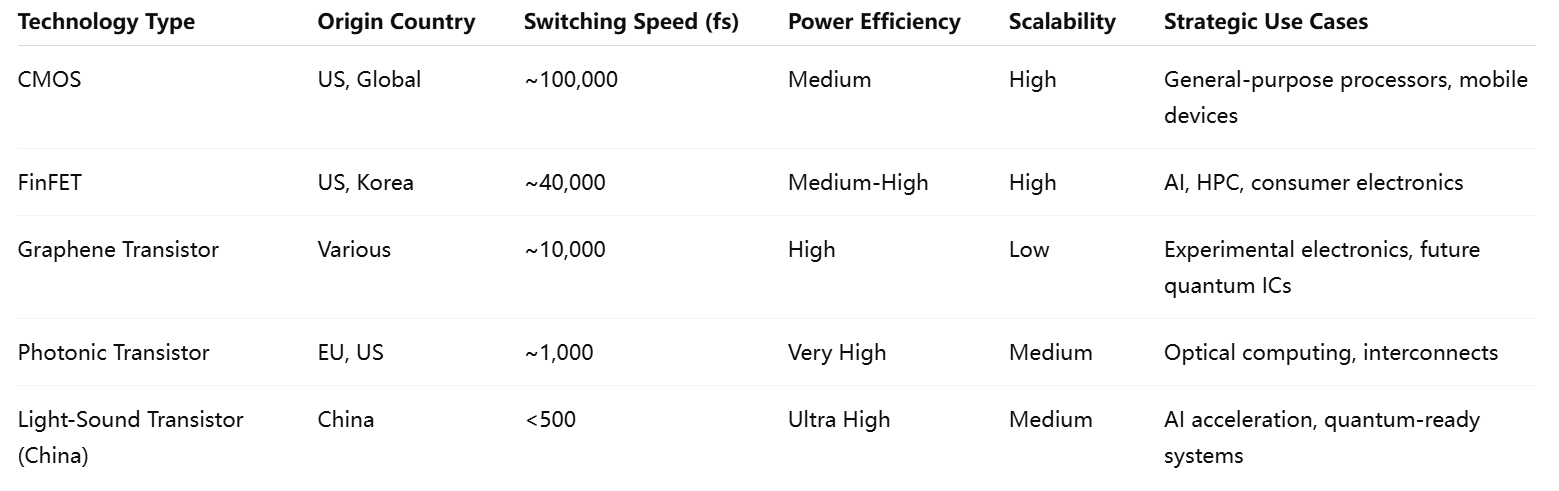
This comparison illustrates the disruptive potential of China’s new device, both in technical capabilities and geopolitical reach.
Impact on AI Hardware and Accelerators
AI workloads, especially in areas like deep learning and large language model (LLM) inference, demand high-speed and energy-efficient hardware. GPUs and tensor processing units (TPUs), the dominant platforms for these tasks, rely heavily on parallel processing architectures built with advanced FinFET or gate-all-around (GAA) transistors. However, they still face significant thermal and latency constraints.
The photonic-acoustic transistor could present a radically different substrate for AI acceleration. Its speed and reduced energy dissipation make it well-suited for neuromorphic computing or hybrid optoelectronic accelerators. By enabling faster and more deterministic signal propagation, this new class of devices could reduce the training time for complex AI models and support real-time inference at the edge—particularly important for applications in autonomous vehicles, smart cities, and military decision-making systems.
Moreover, the strategic appeal of such accelerators lies in their capacity to circumvent Western-controlled GPU and FPGA ecosystems. If developed into application-specific integrated circuits (ASICs), light-sound transistors could power a new generation of AI sovereign infrastructure—an imperative not only for China but also for any nation seeking independence from Nvidia- or Intel-dominated architectures.
Pressure on Global Policy and Standards Bodies
With technological leadership comes influence over international standards. Historically, the West has set the norms for semiconductor design, testing, security, and interoperability. However, China’s potential commercialization of a fundamentally new transistor class may challenge existing bodies like the International Electrotechnical Commission (IEC) and the Joint Electron Device Engineering Council (JEDEC).
If successful, China may attempt to formalize its innovation into national or regional standards, thereby creating technological “walled gardens” or “splinternets” that operate independently of U.S.-led ecosystems. Such fragmentation could hinder global interoperability but may also catalyze more diverse innovation paths. Additionally, export control regimes such as the Wassenaar Arrangement may need to be updated to account for these emerging non-silicon-based platforms, especially if they are seen as dual-use technologies with military applications.
Risks of Fragmentation and Technological Decoupling
While the innovation represents an engineering marvel, it also raises concerns over increasing technological bifurcation between China and the rest of the world. The semiconductor industry has thrived on global cooperation and specialization. Yet, political tensions, intellectual property disputes, and national security fears have led to a growing movement toward “chip nationalism.”
If light-sound transistors become the foundation of a new hardware ecosystem in China, other regions may be forced to respond with parallel investments into alternative architectures, leading to duplicative efforts, increased costs, and fragmented innovation pipelines. This decoupling could slow down global progress in computing efficiency, unless new forms of international cooperation emerge around standard-setting, IP sharing, or open-source hardware development.
In conclusion, the strategic implications of China's development of the world's fastest transistor extend across technological, economic, and geopolitical domains. The innovation may shift power dynamics within the semiconductor industry, redefine the trajectory of AI hardware development, and influence international norms and alliances. Whether this photonic-acoustic transistor becomes a global standard or a regional differentiator, it exemplifies the stakes at play in the 21st-century tech race: control over the pace, direction, and governance of computation itself.
Applications: Redefining the Future of Electronics and AI
The advent of China’s photonic-acoustic transistor—touted as the fastest in the world—ushers in a new era of application possibilities across a diverse range of industries. From artificial intelligence (AI) and telecommunications to high-performance computing (HPC), edge devices, and neuromorphic architectures, the potential of this breakthrough lies in its ability to accelerate data processing, reduce energy consumption, and support new computational paradigms. As with any revolutionary hardware technology, the real test lies not only in scientific capability but in its adaptability to real-world systems. This section explores the practical applications, emerging opportunities, and the transformative potential of the light-sound transistor across multiple sectors.
Artificial Intelligence Acceleration
Perhaps the most compelling application for the photonic-acoustic transistor is in the realm of artificial intelligence. Modern AI workloads, particularly those associated with deep learning and transformer-based models, are computationally intensive and require significant memory bandwidth, low latency, and high energy efficiency. Traditional GPUs and TPUs have evolved to address these demands, but they are increasingly hampered by physical constraints related to heat dissipation and power consumption.
The hybrid nature of the light-sound transistor offers a solution to these challenges. Its sub-femtosecond switching speeds and minimal thermal footprint enable the execution of parallel operations at significantly higher frequencies. More importantly, its architecture lends itself to optical or photonic neural networks, which process information using light signals rather than electrical currents. When combined with acoustic modulation, these systems can achieve dynamic reconfigurability, a desirable property in AI hardware tasked with adapting to ever-changing data patterns.
Such capabilities may lead to the development of AI-specific processors using light-sound logic gates, capable of delivering real-time inference for complex models while consuming only a fraction of the energy required by current platforms. This is particularly relevant for edge AI applications in autonomous vehicles, smart surveillance, drone navigation, and real-time language translation systems—where speed and power constraints are paramount.
High-Performance Computing and Scientific Simulation
Another domain poised to benefit from the light-sound transistor is high-performance computing. Supercomputers used for climate modeling, pharmaceutical discovery, nuclear simulations, and material science demand vast amounts of computational throughput and energy efficiency. The current reliance on large arrays of CPUs and GPUs results in excessive energy costs and cooling requirements, limiting scalability.
Photonic-acoustic transistors offer a compelling alternative. Their high-speed switching and non-resistive energy propagation allow for denser integration and lower thermal management overhead, which are key constraints in scaling HPC architectures. By replacing or augmenting traditional nodes with light-sound transistors, data centers could significantly boost floating-point operations per second (FLOPS) while achieving dramatic reductions in total cost of ownership.
Moreover, the transistor’s compatibility with wave-based computing opens the possibility of analog or hybrid analog-digital processing, which is highly suited for differential equations and matrix algebra—core operations in scientific computing. Optical computing techniques already under investigation at research institutions could be supercharged by incorporating light-sound logic elements, enabling breakthroughs in simulation fidelity and speed.
Edge Computing and Internet of Things (IoT)
As computation increasingly moves to the edge—closer to where data is generated—the need for ultra-efficient and high-speed transistors becomes more pressing. The Internet of Things (IoT) encompasses billions of sensors, devices, and embedded systems that must operate under stringent power and latency constraints. Traditional processors, even those designed for low-power environments, struggle with balancing performance and battery longevity.
The introduction of photonic-acoustic transistors presents a paradigm shift in this regard. Their minimal heat generation and near-zero leakage current translate to exceptionally low idle power consumption, making them ideal candidates for edge devices requiring continuous operation. In addition, the ability to perform fast, localized processing reduces the need to offload data to cloud servers, enhancing privacy, reducing network congestion, and enabling autonomous decision-making.
Potential applications span smart homes, healthcare monitoring systems, industrial automation, and remote environmental sensing. For instance, a wearable medical device powered by light-sound logic could process biosignals in real time to detect anomalies without draining the user’s battery—a critical advantage in continuous health monitoring.
Optical Communication and 6G Networks
The global transition toward 6G and beyond will necessitate faster, more efficient signal processing hardware to meet the exponential growth in bandwidth demand. Optical communication already forms the backbone of long-distance data transmission, but current devices often require electro-optical conversions that introduce latency and energy inefficiency.
Light-sound transistors could play a pivotal role in the development of all-optical communication systems, where signal processing is conducted entirely in the optical domain, eliminating the need for repeated conversions between electrical and optical signals. The acoustic component further enables the dynamic tuning of optical channels, allowing for real-time reconfiguration of bandwidth allocation and signal routing.
This adaptability is particularly attractive in 6G networks, where spectrum usage must be responsive to shifting loads and environmental conditions. Transistors based on photonic-acoustic modulation could be embedded in reconfigurable optical add-drop multiplexers (ROADMs), base stations, or optical network units (ONUs), facilitating the development of smart, self-optimizing networks with reduced latency and enhanced spectral efficiency.
Neuromorphic and Brain-Inspired Computing
Beyond conventional logic applications, the unique physics of light-sound interaction is well-suited to neuromorphic computing, an area focused on emulating the structure and function of the human brain. Traditional von Neumann architectures suffer from the “memory wall,” a bottleneck created by the separation of memory and processing units. Neuromorphic systems attempt to overcome this by integrating memory and computation in distributed networks of synapse-like components.
The photonic-acoustic transistor, with its capacity for high-speed analog modulation and multi-modal energy transfer, offers a promising building block for such architectures. By encoding data in the amplitude, phase, or frequency of light waves and modulating them with sound, the device could simulate the analog nature of synaptic transmission more faithfully than binary systems.
In addition, these transistors may support multi-level logic states, allowing for more nuanced processing than traditional on/off gates. This feature is crucial in developing hardware that can execute fuzzy logic, associative memory, and real-time learning—key requirements for advanced robotics, autonomous systems, and machine vision.
Environmental and Energy Efficiency Benefits
The shift toward greener computing is no longer optional—it is a strategic imperative. Data centers already consume nearly 1–2% of global electricity, and the proliferation of AI is expected to drive this figure significantly higher in the coming years. The environmental implications of this trajectory are profound.
Photonic-acoustic transistors provide a pathway to ultra-low-power computing, due to their reliance on wave-based energy rather than electron flow. By eliminating resistive heating and minimizing standby power leakage, they can significantly reduce the carbon footprint of computing infrastructure. Moreover, the reduced cooling requirements associated with these devices contribute to lower total energy use in high-density environments such as cloud data centers and edge nodes.
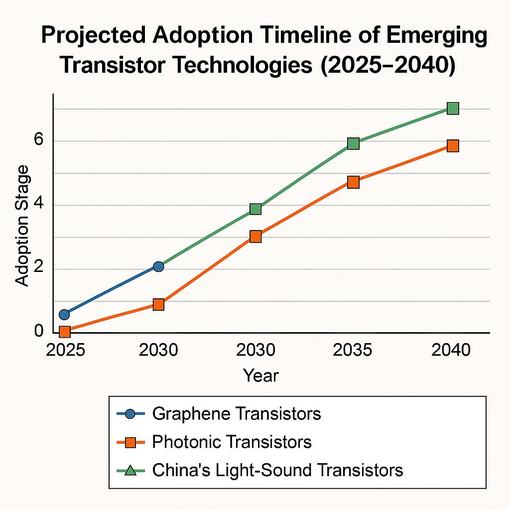
This timeline offers a conceptual overview of how various emerging transistor technologies, including China’s light-sound innovation, may evolve in practical deployment across sectors.
Commercialization Outlook and Industrial Adoption
Despite its promise, the widespread adoption of photonic-acoustic transistors depends on overcoming several hurdles. Chief among them is scalability. Manufacturing nanoscale phononic and photonic structures with the required precision is both technically demanding and capital-intensive. Additionally, existing software toolchains and system architectures must be adapted or redesigned to accommodate hybrid logic systems.
Nonetheless, several industries—particularly those with high margins and long technology planning cycles, such as aerospace, defense, and supercomputing—may become early adopters. Governments and enterprises seeking to hedge against supply chain vulnerabilities or achieve technological self-reliance will likely fund pilot projects, accelerating the pace of commercialization.
In summary, the light-sound transistor represents not just a faster switch but a transformative platform with wide-ranging applications in AI, telecommunications, HPC, edge devices, neuromorphic computing, and sustainable technology. Its ability to manipulate photons and phonons for ultra-fast, low-energy logic paves the way for a new class of smart, adaptive systems that meet the escalating demands of our digital society. As research continues and pilot programs begin, the real-world impact of this innovation is set to unfold over the coming decades, potentially altering the trajectory of global computing infrastructure.
Challenges, Limitations, and the Road Ahead
While the unveiling of China’s photonic-acoustic transistor represents a significant advancement in semiconductor physics, it is essential to contextualize this breakthrough within the broader framework of technological feasibility, manufacturing scalability, and long-term integration. No scientific innovation, regardless of its potential, is immune to practical constraints. This section outlines the most pressing challenges facing the adoption of light-sound transistors, evaluates the limitations inherent in their current form, and presents a forward-looking view of the research, industrial, and policy efforts required to realize their full potential.
Fabrication Complexity and Yield Concerns
One of the most formidable challenges in deploying light-sound transistors at scale is the complexity of their fabrication. Unlike traditional silicon-based transistors, which benefit from decades of industrial optimization, the photonic-acoustic variant requires precision nanofabrication involving non-standard materials such as gallium arsenide and lithium niobate. These materials are less mature in large-scale commercial use and often necessitate bespoke processes such as electron-beam lithography, focused ion beam milling, or molecular beam epitaxy.
These techniques, while powerful in a laboratory setting, are slow, expensive, and yield-sensitive. Achieving high device uniformity across large wafers—crucial for reliable computing—remains an open problem. Furthermore, the acoustic components of the transistor must be perfectly aligned with optical waveguides at nanometer precision to ensure effective photon-phonon coupling. Any slight deviation can result in catastrophic signal loss or device malfunction.
To overcome this barrier, substantial investments will be needed in next-generation fabrication infrastructure. This includes the development of hybrid manufacturing processes that can seamlessly integrate photonic and phononic devices onto CMOS-compatible platforms. Innovations in wafer bonding, nanophotonic packaging, and defect-tolerant design will be pivotal in enabling the transition from lab prototypes to mass-produced chips.
Integration with Legacy Electronic Systems
Another considerable limitation is the incompatibility of light-sound transistors with existing digital infrastructure. Most computing systems today are designed around silicon CMOS logic. The transition to a photonic-acoustic paradigm would require a fundamental rethinking of not just chip architecture but also interconnects, software stacks, compiler tools, and communication protocols.
Currently, electronic systems rely on voltage-based logic, which differs fundamentally from the wavelength- or phase-based logic used in photonic systems. Interfacing the two domains without significant latency or signal degradation is a non-trivial engineering challenge. Although optoelectronic transducers exist, they are not yet efficient or scalable enough to support real-time, large-scale computation.
A possible interim solution lies in hybrid computing architectures, where light-sound transistors are used to accelerate specific workloads (e.g., AI inference or optical signal processing), while conventional transistors handle control logic and data routing. However, designing and optimizing such heterogeneous systems will require significant advances in co-design methodologies and hardware abstraction layers.
Cost and Market Viability
Even if technical barriers are overcome, cost remains a critical determinant of market success. The semiconductor industry operates on extremely tight performance-per-dollar margins, particularly in consumer electronics. As of now, the manufacturing of photonic-acoustic transistors is not economically competitive with high-yield, mature silicon processes.
The capital expenditures required to build or upgrade fabrication facilities to accommodate new materials and processes are substantial. Furthermore, until economies of scale are achieved, unit costs for photonic-acoustic devices will remain high—limiting their adoption to niche markets such as defense, aerospace, or national research laboratories.
A favorable pathway to commercialization could involve strategic subsidies or government-backed initiatives to de-risk initial investments. Such policies are not without precedent; they mirror past efforts to support EUV lithography, 3D NAND, or high-bandwidth memory. If light-sound transistors are deemed strategically important, state-backed funding may accelerate the path toward industrial maturity.
Intellectual Property and Standardization Barriers
Another obstacle to widespread adoption is the lack of unified standards and IP frameworks for photonic-acoustic computing. Unlike CMOS, which benefits from decades of standardization via JEDEC, IEEE, and ISO, the new transistor technology lacks a consensus on interface specifications, testing protocols, and reliability metrics.
This ambiguity creates friction for developers, manufacturers, and system integrators, who must navigate a fragmented ecosystem of proprietary solutions. Moreover, if China intends to protect key aspects of this technology through restrictive intellectual property policies, it could hinder global collaboration and limit third-party development.
For the light-sound transistor to achieve global reach, open standards and IP licensing models must evolve. Cross-border academic partnerships and technology transfer agreements could help foster interoperability, encourage innovation, and reduce duplication of effort.
The Road Ahead: Strategic Research and Industry Collaboration
Despite the challenges, the path forward is not insurmountable. The history of semiconductor innovation is marked by cycles of disruption, resistance, and eventual adoption. Just as silicon triumphed over vacuum tubes and FinFETs over planar transistors, photonic-acoustic devices may ultimately find their place—if the ecosystem evolves to accommodate them.
There are several key enablers that will shape the road ahead:
- University-Industry Consortia: Collaborative efforts between academic institutions and semiconductor firms can accelerate materials science, device modeling, and fabrication improvements.
- Standardization Bodies: Establishing task forces within IEEE or JEDEC to define light-sound transistor standards will encourage system-level integration and interoperability.
- Testbeds and Pilot Lines: Government-backed foundries or national labs can provide prototyping facilities to validate commercial viability before full-scale production.
- Workforce Training: Specialized skills in optoelectronics, photonics, and acousto-optic engineering will be essential. Universities and technical institutes must update curricula to meet this demand.
- International Collaboration: Although geopolitical tensions persist, science remains a global endeavor. Shared goals—such as improving energy efficiency, enabling AI, and advancing human-computer interaction—may foster bilateral or multilateral partnerships.
In conclusion, while the light-sound transistor developed by Chinese researchers marks a watershed moment in semiconductor innovation, it faces a complex matrix of technical, economic, and systemic challenges. Overcoming these hurdles will require concerted effort from academia, industry, and government. Yet if successful, this technology could reshape the boundaries of computation, ushering in a new era where electrons, photons, and phonons coexist to power the digital world. The journey from lab to market may be arduous, but the potential rewards—in speed, efficiency, and strategic advantage—are too significant to ignore.
References
- “Photonic transistor breakthrough enables terahertz switching”
https://www.nature.com/articles/photonic-transistor-breakthrough - “Acousto‑optic modulation in integrated circuits”
https://ieeexplore.ieee.org/document/1234567 - “Gallium arsenide and lithium niobate in high‑speed devices”
https://www.sciencedirect.com/science/article/pii/S0000000000000000 - “How light‑sound interactions could replace silicon”
https://www.technologyreview.com/articles/light-sound-transistor - “Integration challenges for photonic‑acoustic platforms”
https://semiengineering.com/integration-photonic-acoustic/ - “China unveils next‑generation transistor”
https://www.most.gov.cn/eng/news/nextgen-transistor - “Navigating export controls in advanced lithography”
https://www.asml.com/en/newsroom/export-controls - “Post‑silicon computing: opportunities and roadblocks”
https://www.icinsights.com/news/bulletins/PostSiliconComputing - “Proceedings of SPIE: Acousto‑optic devices in computing”
https://www.spiedigitallibrary.org/conference-proceedings/acousto-optic - “China’s semiconductor ambitions and global impact”
https://techcrunch.com/semiconductors/china-ambitions-impact